A Student's Computer Architecture Book I
Contents
1.1 Outline of the book
2 Foundations & Boolean Algebra
2.1 Numeral Systems
2.2 Boolean Algebra
2.2.1 Laws
2.2.2 Theorems
2.3 Boolean Functions
2.3.1 Canonical Representations
2.3.2 Boolean Function Simplification with Karnaugh Maps
3 Logic Gates & Circuits
3.1 NOT, AND, OR, XOR, NOR, XNOR
3.2 Universal Logic Gates
4 Combinational Logic
4.1 Foundational Combinational Circuits
4.1.1 Multiplexer (MUX)
4.1.2 Demultiplexer (DEMUX)
4.1.3 Encoder
4.1.4 Decoder
4.2 Timing
5 Sequential Logic
5.1 Finite State Machine (FSM)
5.1.1 Moore and Mealy FSMs
5.1.2 FSM Simplification
5.2 Clock
5.3 Memory
5.3.1 SR Latch
5.3.2 D Latch
5.3.3 D Flip-Flop
5.3.4 T Flip-Flop
5.3.5 JK Flip-Flop
5.4 Counter
5.4.1 Synchronous Up Counter
5.4.2 Asynchronous Ripple Counter
5.5 Timing
5.5.1 Setup Time Constraint
5.5.2 Hold Time Constraint
6 Let’s Build a Computer!
6.1 Instruction Set Architecture
6.2 Arithmetic
6.3 Logic
6.4 Arithmetic Logic Unit (ALU)
6.5 Random Access Memory (RAM)
6.6 The DX8 Computer
6.6.1 Single-cycle, Multi-cycle, Pipelined Design
6.6.2 Stepper
6.6.3 Controller
6.6.4 Putting everything together!
7 Epilogue
Chapter 1
The Essence of Computing
You may have heard of Babbage’s machine. Yes, Charles Babbage’s Analytical Engine. Well, there was actually his Difference Engine, too, for automated polynomial calculations. Many consider his machine(s) very first computing devices created by human species. However, I would say that the history of computing goes way earlier than that. You’ll say, “of course, there is the Abacus invented somwhere in between 1000-500 BC”. You would be right, but apparently there is this 8 cm-long bone tool made of a baboon fibula that has been used by humans of the Earth as early as 35,000 BCE. “What was its purpose?”, you ask. There are some debates around its purpose, but it is believed to be for counting days and tracking time. But of course, it would not be correct to say the essence of computing started from 35,000 BCE. The tools for computing may have started from that time, but the essence of computing was there way before the tools – when humans used their brains to count or calculate stuff. Computing is not solely about the tools, but about the process that can be carried, by using a computer, a simple calculator, a pen and paper, 8 cm-long bone, human figers, or a human imagination produced by its brain. You see, it can be very abstract to define what really computation is. The tools we invent and use help to achieve efficiency in our computations, that is how fast or energy-saving we are when something is computed. However, the tools do not dictate the absolute rules of computation, and in fact, one could argue that it is the essence of computation that dictates the rules under which the tools need to be operating. Even if there was no human population living on the Earth, the essence of computation would still be there if one looked upon the Earth from the dark cosmos. It is because you would still see the planet moving, animals fighting, trees growing, bees flying, weather changing, waves colliding, and other natural processes that cause the world to move from one state into another. This change of states require spending some energy: in computer science, we see this evergy as the computation itself.

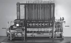
Surely you may think that we have come a long way. Right now, you may be reading this from your personal computer (PC), or your phone, or even from your smart watch. Just imagine how crazy this would be for people living back in the days… They would probably declare you as a witch and try to kill you, or as their technological god and try to protect you. Who knows how the events would have turned up actually?! What’s important for people living in these so-called modern times is to realize the long history of computing and push it even further than where it is standing currently. Doing that is surely a hard task, but if you dedicate yourself enough, you may achieve something significant in your lifespan.
This book is for the beginners who got curious about computers and wondered how they really work at some point in their lives. If you are one of those people trying to get a good grasp of the things that happen inside your computer, I hope that this book will be a friendly mentor that will help you to learn this stuff by yourself. The book will guide you to build your own computer piece by piece. Ideally I would want the reader to gain confidence and be able to build series of computing devices as he/she wishes in the future. You don’t need to be afraid of this seemingly complex and magical-looking devices that we call computers or tablets or phones or smart watches or calculators. Once you understand the foundational principles and basic building blocks that stand behind these devices, you will gain more confidence in building your own – your truly personal computer (TPC).
1.1 Outline of the book
”So, what does it take to build a computer?” you may ask. Well, it takes readding the first \(\approx 70\) pages of this book to understand the fundamentals first:
- Foundations & Boolean Algebra – this chapter will introduce mathematical context that is needed to work with formal boolean logic;
- Logic Gates & Circuits – this chapter will introduce the physical logic components (gates) that can be connected to one another to build real electrical circuits that do something meaningful;
- Combinational Logic – this chapter will show basic but essential circuits that are going to be used quite often in computer building process later on;
- Sequential Logic – this chapter will generalize from the previous types of circuits you know and build more complex circuitry that are very foundational in building many components of a computer;
Then it takes reading the rest \(\approx 15\) pages to put everything together and finally build a custom 8-bit computer:
- Let’s Build a Computer! – finally, this chapter will walk you through the “putting everything together” part, and by the end of it, you will first-hand experience building a computer from scratch;
- Epilogue – the ending chapter will be chill and relax; because you will then be cheered for understanding so much stuff that you didn’t know before and for having the knowledge and courage now to build a computer by yourself if you wanted to do it.
What are you waiting for? Let’s get to it!
Chapter 2
Foundations & Boolean Algebra
2.1 Numeral Systems
Counting is an important and unavoidable part of human life. It is so unavoidable that people have invented multiple different ways of counting things. We put all of these different ways of counting under the name of numeral systems. Let me describe a few of numeral systems. First of all, there is additive numeral systems and then there is positional systems. One example of an additive numeral system is Roman numerals (e.g., VI means 5+1, which is 6). In additive numeral systems, the position of each digit does not affect its magnitude (e.g., even in number IV the calculation goes like -1+5, which is 4; the numbers that are added have the magnitudes 1 and 5). In contrast, in positional numeral systems, the place of each digit affects its magnitude (e.g., 123 in decimal is 100 + 20 + 3 whereas 321 in decimal is 1 + 20 + 300). Since positional systems have been more useful to work with in almost all areas of mathematics and digital logic design, we are going to focus on them from now on.
You see, there are also different positional numeral systems. The difference among positional numeral systems comes from the radix or the base used. The radix (or the base) is the number of elementary symbols that all the numbers of the numeral system are made of. These elementary symbols are also known as the digits. For example, our beloved decimal system uses 10 digits (0, 1, 2, 3, 4, 5, 6, 7, 8, 9), and therefore, the radix is 10. In order to compute the magnitude of the number, each digit in a decimal number is first multiplied by the power of 10 according to the position in which the underlying digit appears within the number and then the results are added, i.e., \(\overline {d_n, d_{n-1}, \dots , d_0}_{10} = 10^n \cdot d_n + 10^{n-1} \cdot d_{n-1} + \dots + 10^0 \cdot d_0\).
Let’s now talk about other radices. There is this numeral systems known as hexadecimal, octal, and binary. The base used in hexadecimal is 16 (i.e., the digits from 0 to 15, inclusively), the base used in octal is 8 (i.e., the digits from 0 to 7, inclusively), and the base used in binary is 2 (i.e., the digits 0 and 1). Similar to the magnitude calculation in the decimal system, here is how the magnitudes are computed (in decimal) for these systems:
2.2 Boolean Algebra
You already probably know what algebra is about. It is about working with expressions that may have numbers, unknowns (or variables), and operators (such as addition, subtraction, multiplication, division, and so on). The algebra that you may have learned in high school is a general kind of algebra than the one we are going to see in this chapter. The algebra you have learned may have an expression as follows: \(3x^2 - \frac {4y}{z} + \frac {2}{7}xz^3\). You may substitute \(x\), \(y\), and \(z\) with different numbers from the real line \(\mathbb {R}\) and then calculate the result of the expression as usual. In boolean algebra we are going to restrict the operations only to addition (\(\mathbf {+}\)), multiplication (\(\mathbf {\cdot }\)), and negation (\(\lnot \) or \('\) or \(\overline {\ }\)); and we restrict the numbers that can be picked/used to a set \(\{0 ,1\}\). This kind of algebra (with the restrictions we introduce) is called boolean algebra. Moreover, we will see all the laws that boolean algebra uses. Although some of the laws are going to overlap with the ones that the ones we used in the high school algebra, there are going to be different laws as well. For example, we have learned in the high school that if we say \(x=1\) and \(y=1\) then the expression \(x + y\) evaluates to 2, but in boolean algebra since there is no number 2 in our set \(\{0, 1\}\) the same expression \(x + y\) or \(1 + 1\) will evaluate to 1. This is very hand-wavy explanation, but we do not need to understand the philosophical reasons behind every law described in this chapter: these laws are the axioms of the boolean algebra, and hence need to be accepted as they are stated. Now, let’s see all the 7 laws of boolean algebra.
2.2.1 Laws
Law 2.1 (Commutativity). The order of operands does not affect the result.
Law 2.2 (Associativity). The grouping of operands does not affect the result.
Law 2.3 (Distributivity). Operations can be factored or expanded.
Law 2.4 (Identity). 0 is additive identity – it means that adding with zero does not give us a different result than the other operand added. 1 is multiplicative identity – it means that multiplying with one does not give us a different result than the other multiplicant multiplied.
Law 2.5 (Idempotent). A different result cannot be obtained by adding or multiplying the same operand with itself. (Just remember that the possible numbers that we can use in binary is 0 and 1; therefore, 0 + 0 = 0 \(\cdot \) 0 = 0 and 1 + 1 = 1 \(\cdot \) 1 = 1 is true according to the laws of boolean algebra.)
Law 2.6 (Complement). Addition with a complement always results in 1. Multiplying with a complement always results in 0.
Law 2.7 (Domination). Adding with 1 always results in 1. Multiplying with 0 always results in 0.
2.2.2 Theorems
Theorem 2.1 (De Morgan). Complement of a sum is equal to the product of the individual complements, and complement of a product is equal to the sum of the individual complements.
Proof. Let’s proceed with proof by exhaustion where we will compute the left-hand side (LHS) and right-hand side (RHS) of the equalities by going through all the possible \(a\) and \(b\) choices from the set \(\{0, 1\}\).
| a | b | \((a+b)'\) | \(a' \cdot b'\) |
| 0 | 0 | \((0 + 0)' = 0' = 1\) | \(0' \cdot 0' = 1 \cdot 1 = 1\) |
| 0 | 1 | \((0 + 1)' = 1' = 0\) | \(0' \cdot 1' = 1 \cdot 0 = 0\) |
| 1 | 0 | \((1 + 0)' = 1' = 0\) | \(1' \cdot 0' = 0 \cdot 1 = 0\) |
| 1 | 1 | \((1 + 1)' = 1' = 0\) | \(1' \cdot 1' = 0 \cdot 0 = 0\) |
Since the third column (LHS of De Morgan equation) and the fourth column (RHS of De Morgan equation) match with each other at every row, we conclude that the theorem is proven to be correct. □
Proof. By using proof by exhaustion,
| a | b | \(a + a \cdot b\) | a | \(a \cdot (a + b)\) |
| 0 | 0 | \(0 + 0 \cdot 0 = 0\) | 0 | \(0 \cdot (0 + 0) = 0\) |
| 0 | 1 | \(0 + 0 \cdot 1 = 0 + 0 = 0\) | 0 | \(0 \cdot (0 + 1) = 0 \cdot 1 = 0\) |
| 1 | 0 | \(1 + 1 \cdot 0 = 1 + 0 = 1\) | 1 | \(1 \cdot (1 + 0) = 1 \cdot 1 = 1\) |
| 1 | 1 | \(1 + 1 \cdot 1 = 1\) | 1 | \(1 \cdot (1 + 1) = 1\) |
Therefore, the theorem has been proven. □
Proof. By using proof by exhaustion,
| a | b | c | \(a \cdot b + a' \cdot c + b \cdot c\) | \(a \cdot b + a' \cdot c\) |
| 0 | 0 | 0 | \(0 \cdot 0 + 0' \cdot 0 + 0 \cdot 0 = 0\) | \(0 \cdot 0 + 0' \cdot 0 = 0\) |
| 0 | 0 | 1 | \(0 \cdot 0 + 0' \cdot 1 + 0 \cdot 1 = 1\) | \(0 \cdot 0 + 0' \cdot 1 = 0\) |
| 0 | 1 | 0 | \(0 \cdot 1 + 0' \cdot 0 + 1 \cdot 0 = 0\) | \(0 \cdot 1 + 0' \cdot 0 = 0\) |
| 0 | 1 | 1 | \(0 \cdot 1 + 0' \cdot 1 + 1 \cdot 1 = 1\) | \(0 \cdot 1 + 0' \cdot 1 = 1\) |
| 1 | 0 | 0 | \(1 \cdot 0 + 1' \cdot 0 + 0 \cdot 0 = 0\) | \(1 \cdot 0 + 1' \cdot 0 = 0\) |
| 1 | 0 | 1 | \(1 \cdot 0 + 1' \cdot 1 + 0 \cdot 1 = 0\) | \(1 \cdot 0 + 1' \cdot 1 = 0\) |
| 1 | 1 | 0 | \(1 \cdot 1 + 1' \cdot 0 + 1 \cdot 0 = 1\) | \(1 \cdot 1 + 1' \cdot 0 = 1\) |
| 1 | 1 | 1 | \(1 \cdot 1 + 1' \cdot 1 + 1 \cdot 1 = 1\) | \(1 \cdot 1 + 1' \cdot 1 = 1\) |
Therefore, the theorem has been proven. □
Proof. By using the distributivity, commutativity, and complement laws,
By case analysis on \(b \cdot c\),
Case 1: \(b \cdot c = 0\) leads the original expression of the theorem to be equal to \(a \cdot c + a' \cdot b + 0 = a \cdot c + a' \cdot b\). Case 2: \(b \cdot c = 1\) leads the original expression to be evaluated to \(a \cdot c + a' \cdot b + 1 = 1\). However, since \(b \cdot c = 1\) also implies that \(b = c = 1\), the previous form in case 1, \(a \cdot c + a' \cdot b = a \cdot 1 + a' \cdot 1 = a + a'\) also evaluates to 1.
From the both cases above, the original expression results in the same boolean values yielded from the expression \(a \cdot c + a' \cdot b\). Therefore, the theorem has been proven. □
Proof. By using proof by exhaustion,
| a | \((a')'\) |
| 0 | \((0')' = 1' = 0\) |
| 1 | \((1')' = 0' = 1\) |
Therefore, the theorem has been proven. □
2.3 Boolean Functions
A boolean function is a regular mathematical function whose domain is the Boolean space \(\{0, 1\}\) and uses only Boolean operations upon the elements of the domain. Another way of looking at it is, anything that takes one or more 0/1 inputs and gives one 0/1 output is a boolean function. So, according to this view, a lookup table with all possible binary patterns on the left-hand-side (LHS) and binary digits on the right-hand-side (RHS) could be considered a boolean function. Just take a look at the lookup table below for a moment. I mean, at the end of the day, this table defines the outputs of ternary function \(f: \{0, 1\}^3 \rightarrow \{0, 1\}\) for all possible 3-bit inputs.
| x | y | z | f(x, y, z) |
| 0 | 0 | 0 | 0 |
| 0 | 0 | 1 | 1 |
| 0 | 1 | 0 | 0 |
| 0 | 1 | 1 | 1 |
| 1 | 0 | 0 | 0 |
| 1 | 0 | 1 | 1 |
| 1 | 1 | 0 | 1 |
| 1 | 1 | 1 | 1 |
The table 2.1 is a representation of a boolean function. It is an exhaustive lookup table essentially, and we call such representation truth table of a boolean function. To state a couple of facts about truth tables, (1) this representation is tabular and not algebraic, (2) it is declarative (i.e., the table states which binary value can be used to substitute \(f(x, y, z)\) for some \(x\), \(y\), and \(z\)) and not imperative (i.e., the table does not state how the outputs are computed by using Boolean logic). Tabular representation is cool, but we would also like to have algebraic representations that are imperative, because we are not planning to use Boolean functions on paper all day long and we actually need to build something in real life that behaves the same as the described boolean function \(f\). Moreover, there is another disadvantage when it comes to representing a boolean function by drawing out its truth table representation: it is exhaustive, i.e., all the possible inputs must be there in the table, making some of even the simple functions with 10 or more binary inputs unskethcable (i.e., practially very painful to sketch because the table needs to have \(2^10 = 1024\) rows). All this being said, now we will see how algebraic representations can be constructed for our beautiful boolean functions.
2.3.1 Canonical Representations
Let’s take a look at our beloved truth table 2.1 for the ternary function \(f : x, y , z \mapsto 0/1\). There are two standartized (canonical) way of representing truth tables: (1) sum of products (SoP) and (2) product of sums (PoS). Let’s see what they are all about…
Sum of Products (SoP)
Sum of products approach to constructing a representation for a given boolean function is all about building a detection mechanism for the inputs for which the function outputs 1. Such detection mechanism can be built out of multiple simpler detection mechanisms that only detect one row. What do I mean by that? Well, imagine that you needed to build a mechanism (that is, essentially another boolean function) that will take an input \((x, y, z)\), and then will output 1 if the input is the one on the third row of the truth table 2.1 and 0 otherwise. For example, I would like to detect the input to the function \(f\) is the one the third row of its truth table, i.e., \(x=0\), \(y=1\), and \(z=0\). Let’s construct a function \(r_3(x, y, z) = \begin {cases} 1, &\text {if } x=0 \text { AND } y=1 \text { AND } z=0 \\ 0, &\text {otherwise} \end {cases}\). I think it must be pretty obvious that \(r_3(x, y, z) = x' y z'\), since to make the condition \(\left [(x=0) \text { AND } (y=1) \text { AND } (z=0)\right ]\) hold, we need to make three subconditions – \(x' = \begin {cases} 1, \text {if } x=0 \\ 0, \text {otherwise} \end {cases}\) for \(x=0\), \(y = \begin {cases} 1, \text {if } y=1 \\ 0, \text {otherwise} \end {cases}\) for \(y=1\), and \(z' = \begin {cases} 1, \text {if } z=0 \\ 0, \text {otherwise} \end {cases}\) for \(z=0\) – hold. Now that we know how to construct a mechanism/function to detect individual rows, it is time to compose these smaller detectors to represent our final function \(f\).
The logic for constructing the detector for the rows for which our function outputs 1 is as follows: we define
Therefore, we can combine 5 detectors to construct a representation for \(f\) as follows: \(f(x, y, z) = r_2(x, y, z) + r_4(x, y, z) + r_6(x, y, z) + r_7(x, y, z) + r_8(x, y, z)\). In other words, we may write \(f(x, y, z) = \sum m(1, 3, 5, 6, 7)\) – sum of minterms (products).
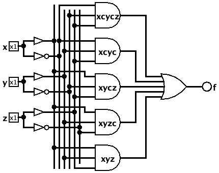
The diagram above illustrates visual representation of the construction of our boolean function \(f\) by using ANDs, ORs, and NOTs. To explain the diagram, the inputs \(x\), \(y\), and \(z\) are shown on the leftmost side. Then each of them are connected to a triangle and another triangle with a circle on its tip: a regular triangle’s output is the same as its input (for example, \(x {\relbar \vartriangleright \rightarrow } x\)) – this is called buffer, the other type of triangle with a circle on its tip outputs its input complement (for example, \(x {\relbar \vartriangleright \hspace {-0.15cm} \circ \hspace {-0.15cm} \rightarrow } x'\)) – this is called negation or complement. The D-shaped drawings, also called AND gates, in the middle column represent logical AND of three inputs that are coming from previous buffers and negations. For example, the D-shaped drawing on the bottom labeled xyz are connected to buffers of x, y, z, and it outputs “x AND y AND z” representing the 8th row from the the function’s truth table where x = y = z = 1. The top AND gate takes its 3 inputs from negatex x, negated y, and z itself (or buffered z), and hence the label “xcycz” – x complement, y complement, z. The last gate on the right side of the diagram that takes 5 inputs from 5 AND gates on its left side and outputs to a wire connected to a circle labeled “f” on its right is called OR gate. It basically adds all of its inputs and outputs the result as the final value of our function \(f\).
Notice that how we have sometimes used complements of variables as an input to AND gate because we cannot really represent “(x = 0) AND (y = 0) AND (z = 1)” by connecting x, y, z to an AND gate on the top: that would have meant that the AND gate outputs 1 when it observes “(x = 1) AND (y = 1) AND (z = 1)” for its inputs and 0 when this observation does not hold. In other words, in order for an AND gate to output 1, it must see that all of its inputs are 1s. Therefore, we used complements x’ and y’ instead to mean that “(x’ = 1) AND (y’ = 1) AND (z = 1)”, which translates to the same “(x = 0) AND (y = 0) AND (z = 1)”. Similarly, the OR gate outputs 0 when it observes all of its inputs as 0s – even if one of the inputs is 1 then it outputs 1, which intuitively makes sense if you think about how the “or” relation in English works.
Product of Sums (PoS)
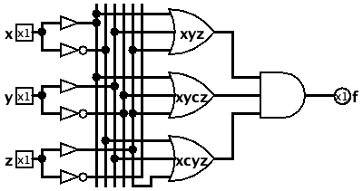
As opposed to the SoP representation, product-of-sums (PoS) is about constructing detection mechanism that recognizes inputs for which the output is 0 in the truth table. With the same logic used in PoS, we could construct three such boolean functions that output 1 only when their input is the one given on the first, third, and fifth rows, respectively. Here are such three functions: \(r_0(x, y, z) = x'y'z'\), \(r_2(x, y, z) = x'yz'\), and \(r_4(x, y, z) = xy'z'\). Now, we could rewrite \(f\)’s definition as follows:
To implement this definition of \(f\), we could first try to detect whether the input appears on one of the rows that make \(f\)’s output 0 by combining three previously built detectors by summing them (SoP): \(r_0(x, y, z) + r_2(x, y, z) + r_4(x, y, z)\). Now this SoP formula has the following definition:
Realize how this definition is the complete opposite of the \(f\)’s definition. Therefore, we could just conclude that
The PoS formula for our function is also written as \(f(x, y, z) = \prod M(0, 2, 4)\) in short – product of Maxterms (sums).
2.3.2 Boolean Function Simplification with Karnaugh Maps
We want the circuits to be minimal and compact, because the less redundant logic (gates) we use in our circuit, the more speed we gain in the propogation of input signals (0s and 1s) in the circuit. Here is one simple example: suppose you build a circuit out of three NOT gates as follows:

If you represent this circuit as a boolean function \(f(x) = x'''\), you can quickly deduce that \(f(x) = x'\) (recall that \(x'' = x\)). Although two representations are semantically the same (they give you the same final output in real life), one is practically slower and more resource-demanding than the other. The first representation \(f(x) = x'''\) requires buying 3 NOT gates from the store (not budget friendly) and runs slower than \(f(x) = x'\), which only requires buying a single NOT gate. All this is to say that minimization of boolean logic is useful and good.
You may wonder if there are other techniques to minimize a given boolean function. There are indeed other techniques beyond the use of boolean algebra laws and theorems (e.g., \(x''=x\), \(x+1=1\), \(x \cdot x = x\), etc.), and one of them is by using so-called Karnaugh maps or K-maps. A K-map is essentially a two-dimensional Euclidean grid that represents all the outputs of a given function to be minimized in a way that neighbouring output values on the grid are the outputs of the function when given very similar inputs. Here’s an example: suppose we have a ternary function \(f(x, y, z) = (x+y+z)(x+y'+z)(x'+y'+z)(x'+y'+z')\). For input 110 (\(x=1,\ y=1,\ z=0\)), \(f(1,1,0) = 0\). So, we say the cell at coordinate \((1,0,1)\) of the 2D K-map grid is \(0\) (output of \(f\) at \((1, 1, 0)\)). Then we are interested in the neigbouring cells located at \((0, 1, 0)\), \((1, 0, 0)\), and \((1, 1, 1)\). \(f\)’s outputs at these locations are, \(f(0,1,0)=0\), \(f(1,0,0)=1\), \(f(1,1,1)=0\). This is how we visually represent the grid with the cell locations (inputs to our boolean function) and the function outputs:
\(\vcenter {\hbox {\diagbox@pict }}\) | 0 1 | |
00 |
|
|
01 | 0 |
|
11 | 0 | 0 |
10 | 1 |
|
Now, we fill the rest of the empty cells of this grid. Notice that how rows are indexed with location/inputs 00, 01, 11, 10 and not 00, 01, 10, 11. This is because we want the neighbouring locations/inputs to be as similar to one another as possible. If you look carefully, going from 00 to 01 makes only a single bit flip, as well as going from 01 to 11, from 11 to 10, and from 10 to 00 back again. However, if the rows were indexed with the “00, 01, 10, 11” order, going from 01 to 10 would make two bits flipped (this is also true for going from 11 to 00 back again), and therefore, the neighbouring locations would not be as close as they are with the “00, 01, 11, 10” indexding. This is called (2-bit) gray codes – (2-bit) binary numbers ordered in a number line such that each consecutive number on the line is only single bit-flip away from the other. For the columns of K-map, we also need to use gray codes. Since there is only single bit \(z\) represented as the column values, any ordering (“0, 1” or “1, 0”) is a valid and gray code compliant; in our table we have used “0, 1” ordering.
\(\vcenter {\hbox {\diagbox@pict }}\) | 0 1 | |
00 | 0 | 1 |
01 | 0 | 1 |
11 | 0 | 0 |
10 | 1 | 1 |
What now, you ask? The last step after filling the grid is to look for prime implicants – a rectangular selection of \(2^{i \in \mathbb {N}}\) number of cells filled with 1s only. Notice that the K-map grid wraps around both horizontally and vertically, so a rectangular selection wrapping over horizontally or vertically is also valid.
\(\vcenter {\hbox {\diagbox@pict }}\) | 0 1 | |
00 | 0 | 1 |
01 | 0 | 1 |
11 | 0 | 0 |
10 | 1 | 1 |
While we do our group selections, we always try to make the largest groups of size \(2^i\) possible. Groups may possible overlap and there is no problem with that. In fact, sometimes we deliberately pick overlapping groups to maximize their sizes as much as possible. The higher \(2^i\) number of 1s we have in our groups, the more compressed our final algebraic representation for the given function will become. Having the two final groups (also known as essential prime implicants) in our K-map example means that we will have two minterms or products in our minimized representation. To construct a product from any given group on the grid, you just need to find the input variables that do not change across the cells within the same group. In our case, for the yellow essential prime implicant, \(x\) and \(z\) do not change, so the product for this group is the multiplication of these invariants converted to boolean value of 1 (by using negations when necessary), \(x'z\). For the green essential prime implicant, the invariants are \(x\) and \(y'\): therefore, the product is \(xy\). Finally, the minimized representation for the function \(f(x, y, z) = xy' + x'z\) will be \(f(x, y, z) = xy' + x'z\).
Chapter 3
Logic Gates & Circuits
A logic gate is a piece of hardware that computes one of basic functions from the boolean logic algebra such as boolean addition, or boolean multiplication, or, boolean negation, or some simple combination of these. Hardware people use these logic gates to construct circuits. First, we’ll see what logic gates there are and then we’ll use these gates in order to build more circuits that have high-level capabilities. Here, you are going to see some basic logic gates that are going to be useful in building many other high-level essential computer components.
3.1 NOT, AND, OR, XOR, NOR, XNOR
The first logic gate is called the NOT gate. NOT gate is to compute a unary boolean negation function, \(\operatorname {NOT}(x) := x'\). Note that we may use \(\overline {x}\) or \(\lnot x\) in exchange with \(x'\) from time to time; all of these notations mean the same thing in this book. The truth table and visual representation for the NOT gate are given below:
| x | \(\operatorname {NOT}(x) := x' = \overline {x} = \lnot x\) |
| 0 | 1 |
| 1 | 0 |

The second logic gate is the AND gate. The AND gate is used to compute binary multiplication in boolean algebra, \(\operatorname {AND}(x, y) := x \cdot y\) or \(xy\) in short. Here’s its truth table on the left and its diagramatic representation on the right:
| x | y | \(\operatorname {AND}(x,y) := x \cdot y\) |
| 0 | 0 | 0 |
| 0 | 1 | 0 |
| 1 | 0 | 0 |
| 1 | 1 | 1 |
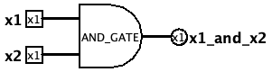
OR is another logic gate that computes binary addition in boolean algebra, \(\operatorname {OR}(x, y) := x + y\). Its truth table and diagramatic representation is given below:
| x | y | \(\operatorname {OR}(x,y) := x + y\) |
| 0 | 0 | 0 |
| 0 | 1 | 1 |
| 1 | 0 | 1 |
| 1 | 1 | 1 |
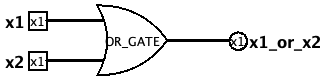
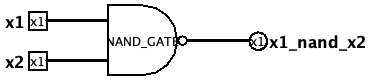
Believe me when I say this: we can already built a lot by using the NOT gate and the AND gate. By a lot, I actually mean everything that can be built by using all the logic gates described in this chapter. Yes, these two gates combined are really universally powerful. But this is the next section’s subject, so let’s keep going on with the different logic gates for now. Engineers have made another dedicate physical gate for this as well: it’s called the NAND gate or the “NOT AND” gate. By combining NOT and AND gates into a single hardware component, one can spend their money only on tons of the NAND gates and then sleep at nights knowing that anything can be built by using this single type of logic gate in his/her basement. Here’s NAND’s truth table and how it looks on the circuittry:
| x | y | \(\operatorname {NAND}(x,y) \text { or } \operatorname {NOT}(\operatorname {AND}(x, y)) := (xy)' = x' + y'\) |
| 0 | 0 | 1 |
| 0 | 0 | 1 |
| 1 | 0 | 1 |
| 1 | 1 | 0 |
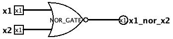
Now, it is time to explore other logic gates that are essentially composition of the ones that we have seen already. The first one we are going to see is the NOR gate that first ORs (addition in boolean algebra) two inputs or operands and then NOTs (negation in boolean algebration) the result. Its name is the abbreviation for NOT-OR: \(\operatorname {NOR}(x, y) = (x + y)'\). Keep in mind that we will prove the universality of the NOR gate later, as well. Below is given its truth table and diagramatic representation:
| x | y | \(\operatorname {NOR}(x,y) \text { or } \operatorname {NOT}(\operatorname {OR}(x, y)) := (x+y)' = x'y'\) |
| 0 | 0 | 1 |
| 0 | 1 | 0 |
| 1 | 0 | 0 |
| 1 | 1 | 0 |
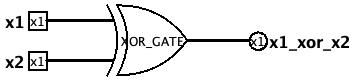
Another type of “OR-ing” two numbers is by using XOR or eXclusive OR. While how the OR gate functions can be translated into the word “or” in English directly, and NOR gate’s behavior can be described by using the words “not or” in English, XOR’s behavior can be translated to “either…or…” wording. XOR is a binary function, so it takes two numbers as inputs: \(x\) and \(y\), let’s say. We say, it outputs 1 if and only if either \(x\) is 1 or \(y\) is 1, but not both. So, here’s its truth table and diagramatic representation:
| x | y | \(\operatorname {XOR}(x,y) \text { or } x \oplus y := x'y + xy'\) |
| 0 | 0 | 0 |
| 0 | 1 | 1 |
| 1 | 0 | 1 |
| 1 | 1 | 0 |
Lastly, we have the XNOR gate that computes “NOT XOR” of two given numbers, \(\operatorname {XNOR}(x, y) := xy + x'y'\). Here’s its truth table and diagramatic representation:
| x | y | \(\operatorname {XNOR}(x,y) := \operatorname {NOT}(\operatorname {XOR}(x, y)) = x'y' + xy\) |
| 0 | 0 | 1 |
| 0 | 1 | 0 |
| 1 | 0 | 0 |
| 1 | 1 | 1 |

These are all the logic gates that we are going to use to build more complex circuitry later on. In fact, we are mostly going to use NOT, AND, and OR gates. The others won’t be used much in this book, but it is still good to know about them. Now, let’s see the universality claims about some of these gates as I promised earlier.
3.2 Universal Logic Gates
We need to ask the following question before we begin: What does it mean for a set of logic gates to be universal all together? The answer is the definition of universality, and here is how it is defined:
Definition 3.1 (Universality of a set of logic gates). A set of logic gates \(\{G_1, G_2, \dots , G_n\}\) is universal if and only if any boolean function can be constructed/implemented only by using the logic gates within this set.
We have already learned about the SoP canonical representation for all boolean functions in the previous chapter. Well, it is already obvious that SoP or Sum-of-Products representation uses Sum and Product among the literals to represent a boolean function. Lastly, a literal can be an input variable or its complement. So, we can conclude that all we need to construct SoP for a given truth table that represents arbitrary boolean function is OR (for construction of Sum), AND (fro construction of Product), and NOT (for construction of complement or negated variable). Therefore, the set \(\{\operatorname {NOT}, \operatorname {AND}, \operatorname {OR}\}\) is universal. □
Proof. To prove that \(\{\operatorname {NOT}, \operatorname {AND}\}\) is a universal set we need to prove that the NAND gate can be used to construct all the gates from another universal set, such as the set \(\{\operatorname {NOT}, \operatorname {AND}, \operatorname {OR}\}\) that we saw earlier. We already have the NOT and AND gates in our candidate set, which are the same with the NOT and AND gates in \(\{\operatorname {NOT}, \operatorname {AND}, \operatorname {OR}\}\). All we need to show that the OR gate in the universal set is constructible by using only NOT and AND gates from our candidate set. Let’s proceed to the construction.
Since only NOT and AND gates can be used to construct all the gates in a universal set \(\{\operatorname {NOT}, \operatorname {AND}, \operatorname {OR}\}\) that we already know of, \(\{\operatorname {NOT}, \operatorname {AND}\}\) is universal. □
Proof. To prove that \(\{\operatorname {NAND}\}\) is a universal set we need to prove that the NAND gate can be used to construct all the gates from another universal set, such as the set \(\{\operatorname {NOT}, \operatorname {AND}\}\) that we saw earlier. Let’s proceed to the constructions.
Therefore, the NAND gate by itself is a universal gate. □
Proof. We will build the NAND gate only by using NOR gate(s) to prove the universality of NOR.
Therefore, NOR gate is a universal gate by itself. □
Chapter 4
Combinational Logic
This chapter makes use of boolean circuits/functions with no “memory” of the past, which is known as combinational circuits. Combinational circuit is a circuit whose output(s) is determined only based on the explicitly given inputs. In other words, the output of a combinational circuit always stays the same as the long as the same input signal is provided. One important concept to be careful about here is the concept of time. Up until now, I did not explitly mention the timing aspect in boolean cirucits, and hence also in boolean functions. For example, take a boolean function \(f(x, y, z) = xy' + x'z\). In this level of abstraction of the representation of \(f\), there is no notion of time: we just say given any \(x\), \(y\), and \(z\), the function evaluates to \(xy' + x'z\). In reality, when you build a physical circuit that implements this function, obviously there is the notion of time as well. Therefore, it would be more realistic to write this function as \(f(x_t, y_t, z_t) = x_t y'_t + x'_t z_t\) where \(x_t, y_t, z_t\) are the inputs provided at time (step) \(t\). Functions of this nature – that is, the output(s) at time step \(t\) only depending on some combination of the inputs provided at the same time step \(t\) – are called combinational functions.
4.1 Foundational Combinational Circuits
This section introduces several combinational circuits that are used quite often while building a typical general-purpose and programmable computer. By general purpose, we mean that any computable function can be programmed into the computer. That is essentially our goal: making a computer to compute our functions for us. I know, sounds exciting, but we have more things to learn first before building our own computer. Now, let’s see about these foundational combinational building blocks of computers.
4.1.1 Multiplexer (MUX)
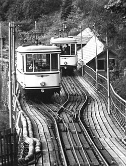
What is a multiplexer? It is a circuit that acts like a switch… like a railroad switch lever. You know the one that decides which train gets to continue with the main railway.
To be more concrete with the multiplexers’ use case, imagine that we have two independent cirucits that do some useful calculations for us. For example, let one circuit take two 1-bit inputs (\(x_1\) and \(x_2\)) and compute their logical AND (\(x_1 \land x_2\)), and let the other circuit take the same 1-bit inputs (\(x_1\) and \(x_2\)) and compute their logical OR (\(x_1 \lor x_2\)); the first circuit is simply made of a single AND gate and the second one is made of a single OR gate, obviously. Now, we would like to somehow select one of the outputs depending on whether we want to compute logical AND or logical OR. In other words, we would like to create a circuit that computes the following mathematical function:
So, if computeOR is 0, we want to get the output of AND gate, and if computeOR is 1, we want to get the output of OR gate. Here is how our unfinished circuit looks right now:
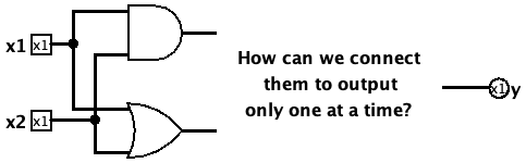
A carefull reader should have felt that something if off about the picture shown above: There is no computeOR input, which was one of the arguments to our function \(f\). So, let’s add that also to our circuit, and now it looks like this:
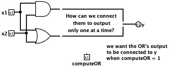
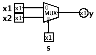
How do we find out a way to connect AND’s and OR’s outputs to the main output wire (connected to \(y\))? To solve this problem, we use a multiplexer or MUX. Here’s how a simple MUX behaves mathematically:
Knowing how MUX behaves mathematically allows us to represent our previous function by using a single MUX as follows: \(f(x_1, x_2, \texttt {computeOR}) = \operatorname {MUX}(x_1 x_2, x_1 + x_2, \texttt {computeOR})\). Figure shown below shows what such a MUX looks like on the left side.
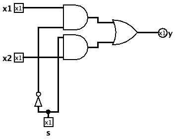
But MUX can be made out of a bunch of AND, OR, NOT gates. All we have to do is to figure out the truth table of the MUX and then find a boolean function for it. This way, we can build the circuit that computes this boolean function. This is what MUX’s truth table looks like:
| \(x_1\) | \(x_2\) | \(s\) | \(\operatorname {MUX}(x_1, x_2, s)\) |
| 0 | 0 | 0 | 0 |
| 0 | 0 | 1 | 0 |
| 0 | 1 | 0 | 0 |
| 0 | 1 | 1 | 1 |
| 1 | 0 | 0 | 1 |
| 1 | 0 | 1 | 0 |
| 1 | 1 | 0 | 1 |
| 1 | 1 | 1 | 1 |
By using the canonical SoP representation, we could easily deduce that \(\operatorname {MUX}(x_1, x_2, s) = x_1' x_2 s + x_1 x_2' s' + x_1 x_2 s' + x_1 x_2 s\). Either by using laws/theorems from boolean algebra that we have learnt or the K-map, we could simply this function further. Let’s try simple algebraic manipulation and see if it takes us somewhere:
The last reduction was done by following the case analysis below:
Since we now know that \(\operatorname {MUX}(x_1, x_2, s) = x_1 s' + x_2 s\), it is easy to understand the MUX’s circuit implemented by using a bunch of AND, OR, NOT gates, as depicted on the figure given previously. Finally, here is what our infamous \(f(x_1, x_2, \texttt {computeOR})\) function looks like:
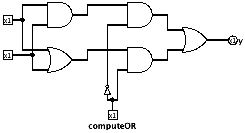
The last thing about the MUX is how many potential inputs there are, only one of which to be forwareded to the final output wire. Up until now, we have only seen MUX with two potential inputs that can be forwarded depending on the select bit \(s\). We are going to call the MUX we have seen 2x1 MUX; where “2x1” means it has 2 non-select inputs (these are the inputs that can potentially be forwarded to the output) and 1 output. But can we have 4x1 MUX? The answer is yes, and it will necessarily have 2 select bits (because one select bit is not enough to select among 4 different input values). One way of building 4x1 MUX is to write out its truth table and come up with boolean function, as we did for 2x1 MUX. Another way of building it is by using several 2x1 MUXs as shown below:
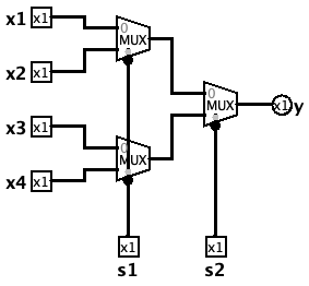
The truth table for this 4x1 MUX is given below:
| \(s_1\) | \(s_2\) | \(\operatorname {MUX}(x_1, x_2, x_3, x_4, s_1, s_2)\) |
| 0 | 0 | \(x_1\) |
| 0 | 1 | \(x_2\) |
| 1 | 0 | \(x_3\) |
| 1 | 1 | \(x_4\) |
So, use your imagination and try to build 3x1 MUX (also write out its truth table for clear understanding), and 8x1 MUX. It is an easy pattern to build any \(2^n\)x1 MUX (for any \(n \in \mathbb {N^+}\)) once you get the intuition; this is also where it becomes obvious that a \(2^n\)x1 MUX must have \(n\) select bits.
4.1.2 Demultiplexer (DEMUX)
We know what MUX is and what it is useful for. It is re-routes only one of its many inputs to the final output wire. Now, what if we have only one input that needs to be routed to only one of many output wires? As 2x1 MUX routes one of 2 inputs to the single output, a 1x2 DEMUX routes single input to one of 2 outputs. Hopefully, you get the naming convention by now.
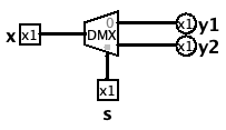
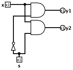
The circuit element for 1x2 DEMUX is depicted on the left side of the picture given above. If you do not understand why 1x2 DEMUX implementation shown on the right side of the same picture works, keep reading; and if you do understand it, you can skip to the next section.
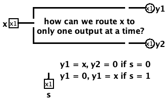
Well, let’s first write out the truth table:
In other words,
By looking at these truth tables, we can conclude that \(y_1 = x s'\) and \(y_2 = x s\). Therefore, the implementation shown below shoud make sense now.
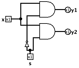
It should be straight forward to see how 1xN DEMUX can be built by using a bunch of 1x2 DEMUXs. In addition, it should also be obvious by now that a 1xN DEMUX must have \(log_2 N\) select bits.
4.1.3 Encoder
Imagine you have a number 3, which you would like to represent in binary. Obviously, a common way would be \(3_{10} = 11_{2}\) or 0011 by using 4 bits. There is another way to represent 3 by using bits: it’s called one-hot encoding and here is how it works:
| Base-10 | Base-2 (using 4 bits) | One-hot |
| 0 | 0000 | 0001 |
| 1 | 0001 | 0010 |
| 2 | 0010 | 0100 |
| 3 | 0011 | 1000 |
In n-bit one-hot encoding representation of numbers, a number is represented by only one turned on (hot bit) and n-1 bits turned off (cold bits). That’s why it is called one-hot encoding and not two-hot encoding. To represent number \(x\) by using one-hot encoding, the hot bit must be at index \(x\) bits left to the rightmost bit in the one-hot representation. For example, 7 is represented as “0010000000” in 10-bit one-hot encoding system.
A \(2^N\)xN encoder is essentially a converter from \(2^N\)-bit one-hot encodings to \(N\)-bit binary numbers. Implementing 2x1 encoder is straight forward. This is how a typical 4x2 encoder could be implemented naively:
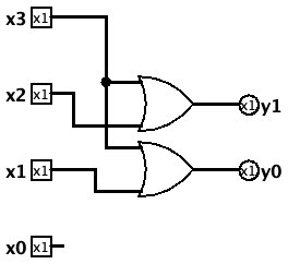
It is a naive implementation in some sense because even though all input bits can be 0 and the output would still be 00, which is not the correct conversion, we have no way of knowing that 0000 input was actually invalid in the first place.
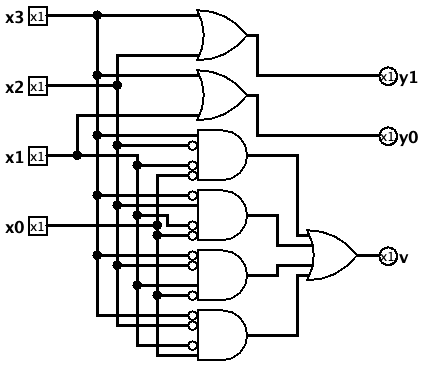
The implementation above still have a problem: it will output 11 for all of the following inputs: input 1000, input 1001, input 1010, input 1011, input 1100, and so on. Now, this behevior is not something that was in a typical encoder’s truth table. That’s why there is another type of encoder that formally accepts this behavior.
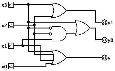
The implementation shown above is called priority encoder because it eliminates the previous problem by converting one-hot encoding to its binary number representation only by using the most significant hot bit. Therefore, even if there are multiple hot bits in the input, it will assume that only the hot MSB is correct and the rest is to be neglected while converting into binary representation.
4.1.4 Decoder
We know what a \(2^N\)xN encoder is and how it works. It translates one-hot encodded representation into a binary representation. What if we wanted to go in the opposite direction, that is, translating a binary representation into one-hot encoded representation? This is exactly what a Nx\(2^N\) decoder does.
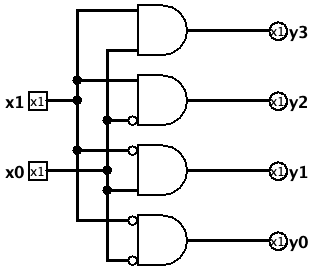
A picture given above is an implementation for a 2x4 decoder. Implementing a Nx\(2^N\) decoder is more straight forward than implementing a \(2^N\)xN encoder because all we have to do is to come up with a single product term for each output of the decoder. For 2x4 decoder, 4 boolean functions can be inferred from the truth table given below:
| \(x_1\) | \(x_2\) | \(y_3\) | \(y_2\) | \(y_1\) | \(y_0\) |
| 0 | 0 | 0 | 0 | 0 | 1 |
| 0 | 1 | 0 | 0 | 1 | 0 |
| 1 | 0 | 0 | 1 | 0 | 0 |
| 1 | 1 | 1 | 0 | 0 | 0 |
Each \(y_i\) is represented in terms of a single product term because there is only one row where each \(y_i = 1\).
4.2 Timing
When we work with boolean logic there is essentially no notion of time in our calculus. It means that we do not take into account the flow of time as we compute boolean functions on paper. It is because there is no meaning to talk about how much second it took us to compute boolean function \(f(x, y, z) = xy' + x'yz + z'\). It is because even though I may need 5 seconds to compute the function’s output, when I tell you that the function’s output for the input \((x=1, y=1, z=0)\) is 1, you know that I have finished my calculation (after 5 seconds). However, within the initial 5 seconds, I could not possibly give you the answer because I wasn’t finished calculating ANDs, ORs, and NOTs. So, you know that the answer I give you is going to be right because you also know that I wouldn’t have given it to you in the first place if I wasn’t done calculating. But this is not how machinery works…
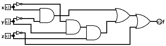
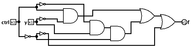
The circuit above is the implementation of the function \(f\). Now, suppose that we would like to compute \(f(1, 1, 0)\) first: so, we need to constantly feed the electrical signals \(5V\), \(5V\), and \(0V\), respectively. As long as we keep feeding these signals to the circuit the answer is going to come out as \(5V\), which is equivalent to the boolean value of 1. Then, the next second we change the voltages accross the input channels so the the input now represents \(x=0\), \(y=1\), and \(z=1\). What do we expect to see at the output? Obviously, still \(5V\) or boolean 1. Is it going to appear immediatly, though? No, not at all. Let’s see why.
It takes some time for the electricity to travel accross wire. The longer the wire, the more time it needs to reach the destination. This is called a delay. I think, this is pretty intuitive thing to think about. For simplicity, let’s assume that for the electricity to flow past the wires and transistors inside each logic gate is fixed at 1ns. We can conclude three things now from this information alone:
- It must have taken ?ns to compute \(f(1, 1, 0)\) in the first place; so, within the ?ns the value at the output wire must have been unreliably because the calculation was not actually done by the circuit.
- After the first ?ns, the output must have been 0 for the new input (0, 1, 1). (oh-ooh! we were expecting to see 1…)
- It was only after the first ?ns, that the circuit’s output must have stabilized at boolean value 1.
Here is the timing diagram to illustrate this process more clearly:
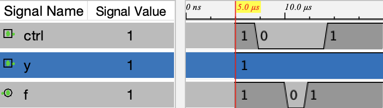
Now, you may get the intuition why timing is important for circuitry. It is because the circuitry does not have a way to be silent until it finished the calculations completely. Instead, it always outputs something: 0 or 1 (this is not completely true, but for the sake of simplicity let’s assume that it is for a moment; thank you). Moreover, if we did not know the least amoung of time it needed to fully calculate \(f(0, 1, 1)\) (that is ?ns in our example), we could have probed the output sooner (for example, after ?ns) and got the wrong result. Such short-term oscillating behavior of circuits is called a glitch, and for us to avoid circuit glitches, we need to know how much we should wait for the circuit’s output to stabilize so that we do not probe the output wire while the circuit is still glitching potentially.
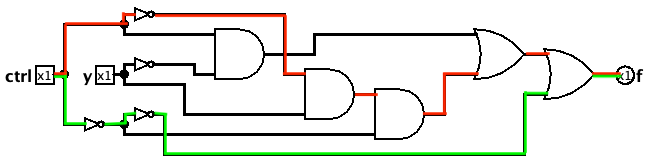
Here I am going to talk about only two types of delays: (1) propagation delay and (2) contamination delay. Propagation delay is the maximum amount of time that electicity needs to travel from input to output. In our example, the propagation delay is \(\text {(AND)} = \)ns Contamination delay is the minimum amount of time that electricity needs to travel from input to output of the circuit. In our example, the contamination delay is \(\text {OR} = \)ns. The longest and shortest paths are shown with red and green colors below to indicate propagation and contamination delays, respectively:
The notion of delays will become more important as we move forward in the book toward building a real functional computer from scratch\({}^*\).
Chapter 5
Sequential Logic
We have learned about the combinational logic: it is a logic to compute output only by using current inputs without taking into account knowledge of the past. In contrast, Sequential logic is a logic that also (may) takes the knowledge of the past into account as well while computing the final output. In this sense, it is more general kind of logic than the combinational logic.
Essential sequential circuits for building a computer are:
- Clock
- Memory
- Counter
Synchronous and Asynchronous circuits. There are two subtypes of sequential circuits: (1) synchronous and (2) asynchronous circuit. Their definitions and differences between them will become more obvious as you learn about the notion of clock and memory.
5.1 Finite State Machine (FSM)
Not all processes are combinational inherently. It means that there are processes that require taking into account some information from the past while computing an output. For example, you can never use solely combinational logic to decide whether a turnstile would have allowed a person to pass through or hold them by knowing person’s current action/input on the turnstile. The set of all possible actions/inputs on the turnstile system is: using-turnstile-pass and turning-turnstile-arm. Well, if I asked you what would happen if the person tried turning-turnstile-arm, you would not be able to answer this questions since there is simply not enough information to be able to answer correctly: you should know whether the person took the using-turnstile-pass, which means buying a pass tiket and then activating/unlocking the turnstile with it, action on the turnstile before trying to turn its arm. Therefore, information about the current time is not enough to determine the future (simply because we do not know if the person paid for the turnstile pass or not). If we tried to build a digital circuit with a single-bit input (that is, if person tried turning-turnstile-arm (input bit 1) or they did not (input bit 0)) and a single output that decided the answer of our question (input bit 1 if the arms turned, and output bit 0, otherwise), we would not be able to make it purely combinational. This is where the notion of states emerge naturally. A state is the abstraction of a persistent storage that keeps track of knowledge of the past. The picture below illustrates what I mean to say:
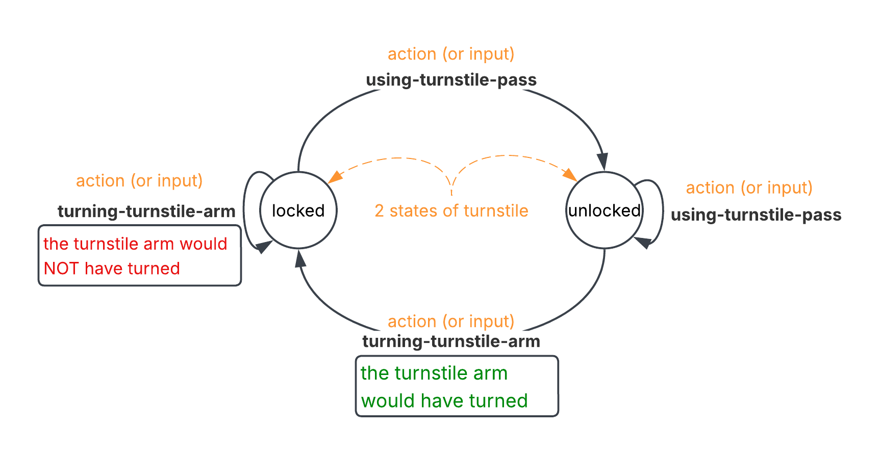
The two circles shown on the diagram above represent the two distinct (and hidden since we do not know whether the turnstile is unlocked or locked just by looking at it without any past knowledge) states of the turnstile: locked or unlocked. The arrows between the states are called state transitions; they represent the current input/action of the person using the turnstile. The turnstile becomes unlocked after purchasing and using-turnstile-pass, and becomes locked after turning-turnstile-arm. If it is already locked and the person insists turning-turnstile-arm, it is obvious that it will keep being in the same locked state. Likewise, if it is already unlocked and the person insists using-turnstile-pass, it will keep being in the same unlocked state. What is more important now is that this state diagram is capable of answering our questions: it is capable of answering the question of “whether the turnstile arm would have turned or not depending on the person’s current action on it” is now within the reach because there are these states that are permenantly embedded in the diagram (as well as in the digital circuit that we are going to build later), and we get to access the hidden information about the past (whether person has used its pass for the turnstile in the most recent past) by keeping track of a single active state in the diagram throughout time. Note that having multiple states are different than having multiple actions because actions need to be provided explicitly while the states are tracked automatically by the circuit.
Understanding the notion of states are really important, so I will give another intuitive example. Imagine you wanted to build a box with 2 buttons, On and Off. Each button is connected to the circuit inside the box through their own wires. Pressing each button would send an electric (high or 1) signal to the circuit inside the box through their corresponding wires as long as the button is pressed, and releasing them would send 0 signal to the circuit as long as they are released.
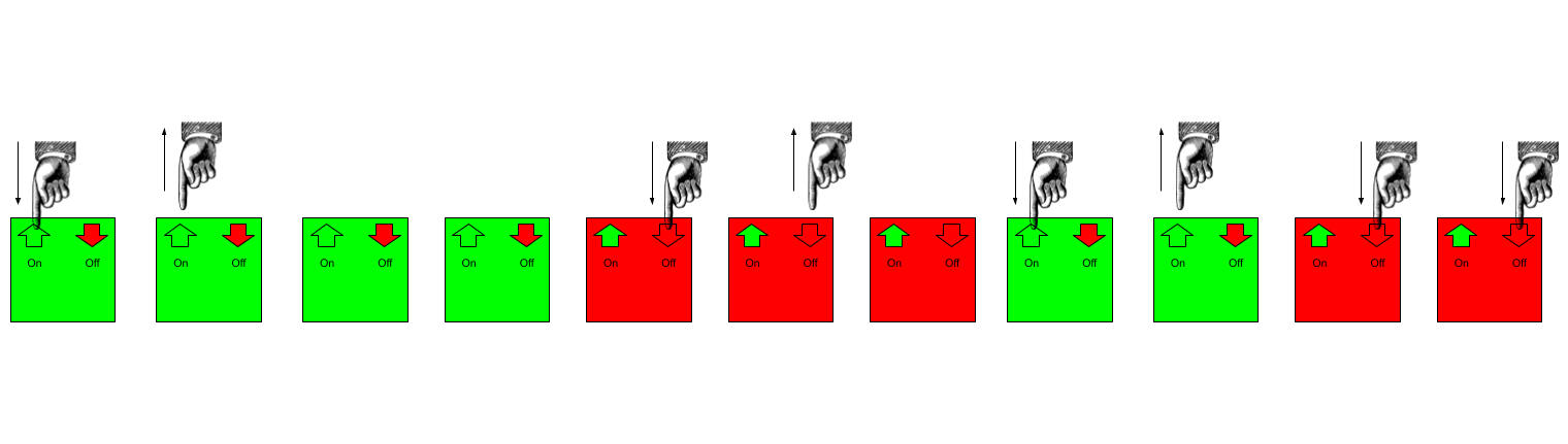
This is how you would like the box to operate:
| Time | 0 | 1 | 2 | 3 |
| Action | “On” pressed | “On” released | (no action) | (no action) |
| Box color | Green | Green | Green | Green |
| Time | 4 | 5 | 6 | 7 |
| Action | “Off” pressed | “Off” released | (no action) | “On” pressed |
| Box color | Red | Red | Red | Green |
| Time | 8 | 9 | 10 | 11 |
| Action | “On released” | “Off” pressed | “Off” pressed | (no action) |
| Box color | Green | Red | Red | Red |
When a button is released, it no longer sends the high signal (input bit 1) to the circuit, and therefore, its input becomes low (input bit 0). Taking no action after releasing a button also performs the same thing since both buttons are in a released state or “0 state”. Since any combinational logic is capable of representing pure mathemetical functions (that is, a mapping is a mathematical function if and only if there exists a single unique \(y\) value for each \(x\) such that \(f(x) = y\)). Due to this “past-independent” behavior, the best combinational circuit we could have made for this box would behave as shown below:
| Time | 0 | 1 | 2 | 3 |
| Action | “On” pressed | “On” released | (no action) | (no action) |
| Box color | Green | X | X | X |
| Time | 4 | 5 | 6 | 7 |
| Action | “Off” pressed | “Off” released | (no action) | “On” pressed |
| Box color | Red | X | X | Green |
| Time | 8 | 9 | 10 | 11 |
| Action | “On released” | (no action) | (no action) | “Off” pressed |
| Box color | X | X | X | Red |
The “On” pressed action represents input (1, 0) and the “Off” pressed action represents input (0, 1); “On” released, “Off” released, (no action) actions represent input (0, 0), and we do not allow pressing both buttons simultaneously, making (1, 1) input impossible. Since releasing each button, as well as performing no action after the release, send the input (0, 0) to the circuit inside the box through the wires connected to the “On” and “Off” buttons respectively, we would not be allowed to map these inputs to different outputs under the law of combinational logic (recall that there must be exactly one \(y\) value for input (0, 0) for any pure combinational function). This is shown in the table above by marking the output for (0, 0) input with X symbol. So, if we say let X be the Red light, then time steps 1, 2, 3, 8 would not produce the expected behavior of this mystical box that we wanted to build; and if we say let X be the Green light, then time steps 5, 6, 11 would not match with the expected behavior.
By going through the two examples provided above, one can understand the problem: using combinational logic for certain types of tasks is just not going to cut it! We need something more powerful, and that is obviously sequential logic. Finite state machine or (FSM) is a machine that performs sequential logic by using its sequential circuitry. The reason we call it “finite state” is because any FSM’s state diagram must consists of a finite set of states. There are two main types of FSMs: Moore FSM and Mealy FSM. We are going to learn more about them through our mystical box example.
5.1.1 Moore and Mealy FSMs
There are two main types of FSMs as mentioned previously. Both types (Moore and Mealy) of FSMs are pretty much the same: they use nodes to represent states and arrows to represent transitions between the states. The main difference between them is how they output something. Moore FSMs output a value from the next active state, but Mealy FSM output upon transitioning to the next state. Let’s see what this really means.
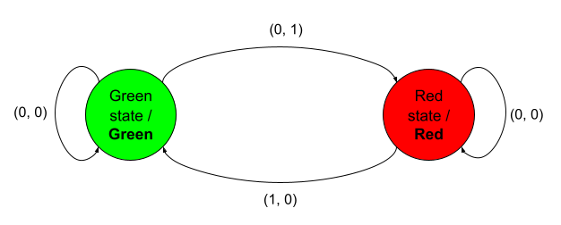
The state diagram shown above is a Moore FSM for our mystical box example. Each node contains two pieces of information in it: (1) state’s name and (2) output value. Since this is a Moore machine, output values are written inside the states with the following convention: [STATE NAME] / [STATE OUTPUT]. One important thing here is that we also must know the initial state that is active. Let’s suppose that the initial state was the “Green state”, and the input was (0, 1) - that is, “On” released and “Off” pressed. The system will transition to the next active state upon receiving this input, and the active state will be the “Red state” with “Red” output. After the Moore machine transitions from the “Green state” to the “Red state”, it will output “Red”, meaning that the box’s color will be red. While it is in the “Red state”, performing (0, 0) – “Off” released, (no action), or “On” released – will transition back to the same “Red state”, resulting with the same “Red” color output. Now, let’s see the Mealy version of this machine.
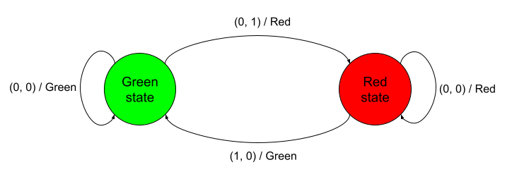
The state diagram above is the Mealy version of our mystic box. The only difference is that it is not the states that output “Green” or “Red”, but rather the transitions/arrows. In the Mealy FSM representation, if the currently active state is the “Red state” and the input is (1, 0) – “On” pressed, “Off” released“ – the machine will output ”Green“ first and then transition to the ”Green state“. Hopefully, these examples made it easier for the readers to informally understand the difference between Moore and Mealy machines. Even though in this simple mystic box example, the difference was pretty much in the written representation of the state diagrams for these two types of FSMs, there are cases where switching from one type of FSM to another reduces or increases the number of states, and therefore, simplifies or complicates the state transitioning logic. Now, we will see how we can simplify unnecessarily complicated state diagrams, resulting in easier and cheaper construction of Moore/Mealy FSMs in practice.
5.1.2 FSM Simplification
For simplifying FSMs, we will use tabular representation instead of the diagramatic ones given as examples previously. Let’s consider the following Moore FSM below:
| State | Input | Next state | Output |
|
a | 0 | b |
1 |
| 1 | c | ||
|
b | 0 | b |
0 |
| 1 | d | ||
|
c | 0 | b |
1 |
| 1 | c | ||
|
d | 0 | b |
0 |
| 1 | c | ||
|
e | 0 | b |
1 |
| 1 | a | ||
Here are the rules to simplify Moore machine:
- Find two states p and q such that output of p = output of q, and p \(\xrightarrow {x}\) s and q \(\xrightarrow {x}\) s for all (x, s) pairs.
- When such two states exist, they are equivalent – remove q and replace all of its occurances in the table with p.
- Repeat the same process from start until no two equivalent states are found.
Let’s now try to simplify the Moore FSM. The first thing you may notice that the states a, c, and e have the same output value, which is 1. However, only a and c transitions to b on input 0 and c on input 1. Therefore, these two states are (semantically) equivalent. Let’s remove the third row from the table and replace all occurances of c with a as shown in the table below:
| State | Input | Next state | Output |
|
a | 0 | b |
1 |
| 1 | a | ||
|
b | 0 | b |
0 |
| 1 | d | ||
|
d | 0 | b |
0 |
| 1 | a | ||
|
e | 0 | b |
1 |
| 1 | a | ||
From the table above you may notice that the states a, d, and e transition to b on input 0 and to a on input 1. However, only a and e output the same value, which is 1. Therefore, these two states are equivalent. Finally, the simplified Moore FSM, which still has the same input-output behavior, is given on the table below:
Now, let’s consider the following Mealy FSM below (different than previous Moore machine):
| State | Input | Next state | Output |
|
a | 0 | b | 1 |
| 1 | c | 1 | |
|
b | 0 | b | 0 |
| 1 | d | 1 | |
|
c | 0 | b | 1 |
| 1 | c | 1 | |
|
d | 0 | e | 0 |
| 1 | c | 1 | |
|
e | 0 | e | 0 |
| 1 | a | 1 | |
Here are the rules to simplify Mealy machine:
- Find two states p and q such that p \(\xrightarrow {x/y}\) s and q \(\xrightarrow {x/y}\) s for all (x, s, y) pairs.
- When such two states exist, they are equivalent – remove q and replace all of its occurances in the table with p.
- Repeat the same process from start until no two equivalent states are found.
Let’s start simplifying. Look at the states a and c. Both of them have the same (0, b, 1) and (1, c, 1) pairs. Since they are equivalent, let’s remove the state c and replace all of its other occurences in the table with a. Now we get the table shown below:
| State | Input | Next state | Output |
|
a | 0 | b | 1 |
| 1 | a | 1 | |
|
b | 0 | b | 0 |
| 1 | d | 1 | |
|
d | 0 | e | 0 |
| 1 | a | 1 | |
|
e | 0 | e | 0 |
| 1 | a | 1 | |
Let’s now look at the states d and e. They have the same (0, e, 0) and (1, a, 1) pairs. So, let’s replace the state e with the state d.
| State | Input | Next state | Output |
|
a | 0 | b | 1 |
| 1 | a | 1 | |
|
b | 0 | b | 0 |
| 1 | d | 1 | |
|
d | 0 | d | 0 |
| 1 | a | 1 | |
The table given above is the final compressed and simplified version of our original Mealy FSM. Both FSMs (original one and the minimized one) have the same input-output behavior for all possible input sequences. This is important for ensuring that the reductions and simplifications we do in an FSM do not alter its behavior semantically.
5.2 Clock
This section will be about something that we all use in our everyday lives. It orchestrates all of us, all at once. It is called clock. Clock is also an important part of the computer architecture: it orchastrates the different components within the computer. However, a clock inside a computer looks very different than the clock we have used to use.
Humans use 12-hour or 24-hour format clocks. For example, in 12-hour wall clock, there are 12 numbers from 1 to 12, and the clock head spins “clockwise” from 1 to 12 and then starts from 1, hypothetically in a never ending infinite loop… Computers use 2-hour format, instead: the clock has two numbers 0 and 1; the clock oscillates between these two numbers. In contrast to the fanciness of the good old clock that we all know and love, the clock used in a computer architecture looks like this:
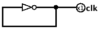
Simple and easy, right? I hope it automatically makes sense for the reader why having a single self-wired NOT gate gives us what we want. It gives us the oscillating OFF-ON-OFF-ON-OFF-ON-… signal. Here is what its timing diagram looks like:

This particular timing diagram given above illustrates the oscillations of a 1 \(\mu \)Hz (frequency) clock, meaning that the clock period is 10 \(\mu \)s.
5.3 Memory
Up until now you have learned about building digital circuits that output some boolean value given an n-bit input. What if we wanted to store the output of a circuit inside somewhere so that we can look it up later when we need it? Well, you guessed it right: it is for this purpose that we need to build a memory component. But… what is memory anyway? Without going to far into the rabbit holes of philosophy, memory is kind of a thing that just persists over time even when the environment around that thing changes. It sounds intuitive to believe, isn’t it? Now, bare with me: if we were able to build a circuit that preserves its output no matter what the inputs are then this piece of circuit may be used as a memory. If we think with a little more care, we can already understand the problem with this circuit: it never allows us to put something in its output through the inputs somehow; it just memorized whatever the random garbage values in its output upon construction. So, we better update our view of the memory systems. Okay, let me try one more time: A memory… a memory is something that gets updated only on certain contexts and gets preserved on all other contexts. With this view of the memory, we can now imagine a circuit that changes its 1-bit output to
- LOW when the input is (0, 1),
- HIGH when the input is (1, 0),
- retains its previous output when the input is (0, 0).
So, we may naturally agree on the convention that the input signal semantically represents (memorize-1, memorize-0): (1, 0) means the circuit must memrize and remember boolean value 1, (0, 1) means the circuit must memorize and preserve boolean value 0, and (0, 0) means nothing new needs to be memorized and therefore the old memorized value must be kept as it is. The input (1, 1) is special. It is special in a sense that it does not make any sense logically in our convention: we cannot expect the circuit to memorize both boolean value 1 and 0 at the same time since it has only a single-bit memory. Here is how this hypothetical circuit would behave over the valid inputs (0, 0), (0, 1), (1, 0):
| Time step | 0 | 1 | 2 | 3 | 4 |
| Input | (1, 0) | (0, 0) | (0, 0) | (0, 1) | (0, 0) |
| Output | 1 | 1 | 1 | 0 | 0 |
But wait! This looks like the mystic box’s behavior from the first section where FSMs were introduced. It turns out that this is exactly the behavior of that mystic box with two buttons; except that here “On” button stands for “memorize-1” and “Off” button stands for “memorize-0”, and “Green” output is represented by boolean value 1 and “Red” output is represented by boolean value 0. Recall that for the mystic box, it also didn’t make any sense to press both “On” and “Off” buttons simultaneously since the box could output only one color (“Green” or “Red”) at a time. Having said this, we now know that the mystic box we saw can actually be used as a simple memory component. Let’s write down the truth table for this mystic memory box:
|
|
| \(\mathbf {Q'_{t+1}}\) | ||||||
| 0 | 0 | \(\mathbf {Q_t}\) | \(\mathbf {Q'_t}\) | ||||||
| 0 | 1 | 0 | 1 | ||||||
| 1 | 0 | 1 | 0 | ||||||
| 1 | 1 | - | - | ||||||
From the truth table above we can clearly see that the output of this circuit, which seems to possess one-bit memory, the output \(\mathbf {Q_{t+1}}\) may be equal to the output value from the past \(\mathbf {Q_t}\) when the input is (0, 0). This implies that the circuit cannot be purely combinational because at certain moment in the future, say \(t+100\), the input (0, 0) may be mapped to the output \(Q_{99} = 0\) and in others, say \(t+200\), the same input (0, 0) may be mapped to the output \(Q_{199} = 1\). Since purely combinational cirucits cannot map the same input to different outputs, this circuit must be sequential. Now, let’s see how we could actually build a sequential circuit for this 1-bit memory, called SR latch.
5.3.1 SR Latch
Set-Reset or SR latch is what the mystic box from the first section of this chapter represented informally. You have seen how this behavior exactly matches with the behavior of a very simple 1-bit memory component that can update its memory upon receiving certain inputs ((0, 1) and (1, 0)) and preserve the old 1-bit value upon receiving another input ((0, 0)). So, we can control what’s kept in the memory without explicitly knowing what’s kept in it. For example, if we wanted to preserve the currently memorized boolean value in the next time step \(t+1\), we would provide the (0, 0) input at the time step \(t\), and if we wanted to update or memorize a new value 0 or 1, we would provide the (0, 1) or (1, 0) input, respectively.
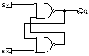
It turns out that it is really simple to build a sequential circuit for SR latch. The circuit is given on the diagram above. It essentially has two NAND gates and two NOT gates (one for each input bit Set and Reset). The NAND gate on top outputs the thing that’s kept on the memory currently - Q. In contrast, the NAND gate on bottom outputs the opposite of that thing - Q’. Now, go ahead and check whether the previous truth table that we saw for this SR latch makes perfect sense: verify the outputs on the truth table by pushing the inputs through the SR latch’s circuit.
| S | R | \(\mathbf {Q_t}\) | \(\mathbf {Q_{t+1}}\) | \(\mathbf {Q'_{t+1}}\) | Valid? |
| 0 | 0 | 0 | 0 | 1 | Yes, \(\mathbf {Q_{t+1} = Q_t \neq Q'_{t+1}}\). |
| 0 | 0 | 1 | 1 | 0 | Yes, same as above. |
| 0 | 1 | 0 | 0 | 1 | Yes, \(\mathbf {Q_{t+1} = 0 \neq Q'_{t+1}}\). |
| 0 | 1 | 1 | 0 | 1 | Yes, same as above. |
| 1 | 0 | 0 | 1 | 0 | Yes, \(\mathbf {Q_{t+1} = 1 \neq Q'_{t+1}}\). |
| 1 | 0 | 1 | 1 | 0 | Yes, same as above. |
| 1 | 1 | 0 | 1 | 1 | No, \(Q_{t+1} = Q'_{t+1}\). |
| 1 | 1 | 1 | 1 | 1 | No, \(Q_{t+1} = Q'_{t+1}\). |
Let’s go through a couple of the rows from the truth table. Suppose the input is (\(S=1\), \(R=0\)) and the previously memorized value is \(Q_t = 0\). Then, we can compute \(\mathbf {Q_{t+1}}\) for the next time step as follows:
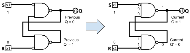
Now, suppose that the input is (0, 0) and we have previously update the latch to store 1. Then this is what happens in the next time step:
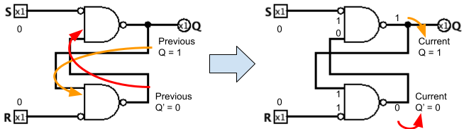
If you go through all of the possible inputs from listed in the truth table, you will verify the outputs mentioned. By doing this you will also see that the \(\mathbf {Q_{t+1}}\) and \(\mathbf {Q'_{t+1}}\) become 1 when the input is (1, 1) and therefore, leads to metastability when the input suddenly switches to (0, 0). When \(S_{t-1} = R_{t-1} = 1\) and then \(S_t = R_t = 0\), it depends on the speed in which one of the either input (\(S_t\) or \(R_t\)) reaches to the NAND gate before the other one does, and then the output will settle either in 0 (if \(R_t\) reaches NAND faster) or in 1 (if \(S_t\) reaches NAND faster). Since it is not up to us to deterministically tell whether \(Q_t = 1\) will be preserved in the next time step when \(Q'_t\) is also 1, providing the (1, 1) input is not a reliable way of storing boolean value 1.
5.3.2 D Latch
You have learned about the SR latch, which is a very basic but essential memory component. Now, we are going to use this basic building block to build more complex but also useful piece of memory circuitry. This one is called D latch and here is how it works: we provide two-bit input (data, enable) to the D latch, and if enable bit is 0 then the previously memorized value at \(\mathbf {Q_t}\) is preserved for the next time step \(t+1\), otherwise (when enable is 1) the memory is updated with the value of the data bit provided at time step \(t\). Check out the truth table for D latch below:
| \(D_t\) | \(E_t\) | \(Q_{t+1}\) | \(Q'_{t+1}\) |
| 0 | 0 | \(Q_t\) | \(Q'_t\) |
| 1 | 0 | \(Q_t\) | \(Q'_t\) |
| 0 | 1 | 0 | 1 |
| 1 | 1 | 1 | 0 |
Since we do not want to start from scratch, we would like to use the SR latch to build the D latch. Now, the question is how can we decide what inputs should be provided to an SR latch so that it acts like the D latch? To answer this question, let’s imagine the following scenario first. Suppose that you tell me you have got a D latch in your pocket and you ask me to test you without seeing or touching your D latch. For me to know whether you are lying or not, I can give you random input values from the D latch’s truth table and ask you about the output of the D latch in your pocket. If what you say D latch outputs given my inputs do not match with the expected output values from the truth table, then I will know that you are lying.
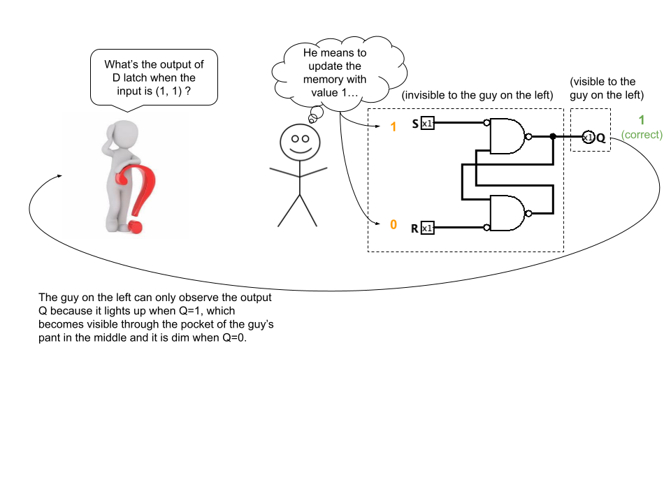
You (the guy in the middle) will act like the interface for the SR latch in your pocket, and through this interface I (the guy on the left) will get the impression that I am actually working with a D latch. So, a D latch is essentially You + SR latch in your pocket. Let’s see the complete truth table for the SR latch interface:
| D latch input | Corresponding SR latch input | Output
| |||
| D | E | S | R | \(Q_{t+1}\) | \(Q'_{t+1}\) |
| 0 | 0 | 0 | 0 | \(Q_t\) | \(Q'_t\) |
| 1 | 0 | 0 | 0 | \(Q_t\) | \(Q'_t\) |
| 0 | 1 | 0 | 1 | 0 | 1 |
| 1 | 1 | 1 | 0 | 1 | 0 |
From the truth table above you could derive the following boolean functions for S and R inputs to the SR latch: \(S(D, E) = DE\) and \(R(D, E) = D'E\). Building this circuit that outputs S and R values given D and E values essentially replaces you (the guy in the middle acting as an interface for the SR latch) and allows us to build the D latch circuit. Here’s how this can be implemented by using SR latch and a couple of AND gates:
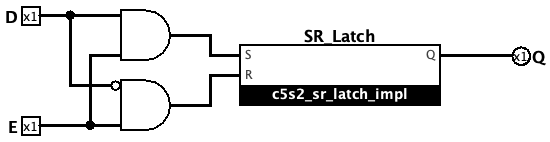
One last thing to note is that there is not invalid inputs when we use a D latch. Each input is valid and has a particular meaning. This is really nice if you want to avoid any uncertainties in your boolean logic when it gets complex. It is especially useful to prove things about the behavior of complex circuitry as well as to debug one when things go sideways.
5.3.3 D Flip-Flop
You have seen how the D latch works: as long as the enable input is high, the latch becomes transparent, i.e., \(Q_{t+1} = D\). To make it opaque, we have to turn off the enable bit after setting the correct data bit. Here is how a proper functioning of a D latch would look like in real life:

If we hook the raw clock output to the enable bit of a D latch, then the setup and hold times would be violated. What’s proven to be useful in practice is to latch a new value once in every clock rising or positive clock edge. The memory components that react to the edge (i.e., transitioning from LOW to HIGH or from HIGH to LOW), as opposed to the stable HIGH input, is called flip-flops. This is as shown on the timing diagram of positive edge-triggered D flip-flop:

A D flip flop can be implemented by using two ordinary D latches and a NOT gate as follows:

Let the circuit diagram above sink in for a moment. There are 2 D latches: the one connected to the data signal D is called master latch and the one connected to the output of the master latch is called slave latch. The idea is as follows: since this is a positive-edge triggered D flipflop, when the clock is low – the master latch becomes transparent when the clock is low (the enable signal for the master latch becomes 1 due to the NOT gate) and the slave latch becomes opaque; when the clock is high – the master latch becomes opaque and the slave latch becomes transparent, updating its output with whatever was latched into the master latch when the clock signal was still low. This transitioning (i.e., master latch storing data when clock is low and slave latch storing master’s output when clock is high) makes the whole circuit act as if it stores the data signal during the positive clock edge. Here is how the timing diagram for both master and slave latches in a D flip flop may look like in practice:

Now, let’s add a cherry on top of the cake by building an asynchronously resettable D flip flop. Resettable means we can reset the memory (set the Q value to 0), and asynchronously resettable means this operation will reset the memory regardless of the clock – whether it is high or low or transitioning from low to high (positive edge) or transitioning from high to low (negative edge).
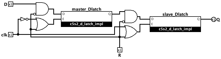
Here’s the truth table for asynchronously resettable D flipflop:
| Reset | Clk | D | \(Q_{t}\) |
|
R=0 | 0 | d | \(Q_{t}\) |
| \(\nearrow \) | d | d | |
| 1 | d | \(Q_{t}\) | |
| \(\searrow \) | d | \(Q_{t}\) | |
| R=1 | x | x | 0 |
5.3.4 T Flip-Flop
Another simple flip flop that is commonly used in counter design is T flip flop. We have not seen counters yet, but we will in the section 5.4.
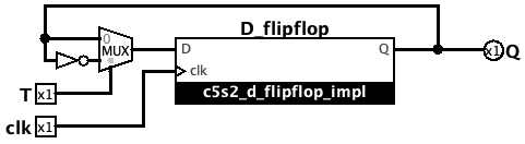
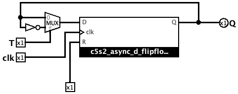
5.3.5 JK Flip-Flop
JK flip flop is another memory unit that has the following truth table:
| Clk | J | K | \(Q_{t+1}\) |
|
\(\nearrow \) | 0 | 0 | \(Q_t\) |
| 0 | 1 | \(0\) | |
| 1 | 0 | \(1\) | |
| 1 | 1 | \(Q'_t\) | |
| \(1/\searrow /0\) | x | x | \(Q_t\) |
Here is how a JK flip flop can be implemented by using a D flip flop and a 4x1 MUX:
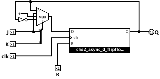
5.4 Counter
0… 1… 2… 3… An n-bit counter is a unit that counts up/down after each clock cycle, outputting an n-bit binary number. For example, here’s a truth table for 3-bit up counter that counts by incrementing previous output and down counter that counts by decrementing it.
| Clk | \(Q^\text {up/down}_t\) | \(Q^\text {up}_{t+1}\) | \(Q^\text {down}_{t+1}\) |
| \(\nearrow \) | 000 | 001 | 111 |
| \(\nearrow \) | 001 | 010 | 000 |
| \(\nearrow \) | 010 | 011 | 001 |
| \(\nearrow \) | 011 | 100 | 010 |
| \(\nearrow \) | 100 | 101 | 011 |
| \(\nearrow \) | 101 | 110 | 100 |
| \(\nearrow \) | 110 | 111 | 101 |
| \(\nearrow \) | 111 | 000 | 110 |
| \(1/\searrow /0\) | q | q | q |
Notice how the up counter’s output \(Q^\text {up}_{t+1}\) wraps around and becomes 000 when it reaches the highest 3-bit binary number 111 (7 in decimal) and how the down counter’s output \(Q^\text {down}_{t+1}\) becomes 111 when the ouptut reaches the smallest 3-bit binary number 000 (0 in decimal). This is not a bug – it’s actually a feature and we will see why when we build our computer!
There are two types of counters regarding their circuit-level clock connections: synchronous and asynchronous counters. Now, you will see how these two types are different from each other.
5.4.1 Synchronous Up Counter
Synchronous counter is a counter that uses clock to update all of its internal registers simulateneously at the same raw clock edges. Calling this type of circuit synchronous makes sense because a single global clock orchastrates the update times for all the memory units inside, and therefore, we say that all units are in sync with the clock. Here is one a 3-bit up counter could be built in practice:
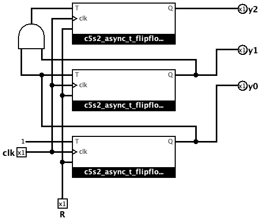
5.4.2 Asynchronous Ripple Counter
Asynchronous counter, as opposed to the synchronous one, may use raw clock signal for updating some of its internal registers and another signal for other registers. This implies that the updating of the all internal memory units does not happen at the same time as the clk signals to different flip-flops come from different sources. One such famous counter is called a ripple counter and here is how it can be implemented:
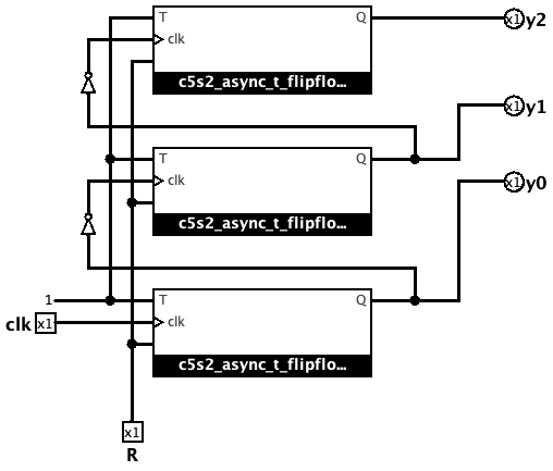
Let’s analyze the circuit above with a bit more care and see why it is called an asynchronous ripple counter. Before starting the analysis, just remember that the \(\nearrow \) notation is used for the \(0 \rightarrow 1\) clock transitioning, and these two notations are exchangeable.
| t=0 | t=1 | t=2 | t=3 | t=4 | t=5 | t=6 | t=7 | t=8 | ||
| clk | \(0 \rightarrow 1\) | \(0 \rightarrow 1\) | \(0 \rightarrow 1\) | \(0 \rightarrow 1\) | \(0 \rightarrow 1\) | \(0 \rightarrow 1\) | \(0 \rightarrow 1\) | \(0 \rightarrow 1\) | ||
| \(\text {clk}_0\) | \(\nearrow \)1 | \(\nearrow \)1 | \(\nearrow \)1 | \(\nearrow \)1 | \(\nearrow \)1 | \(\nearrow \)1 | \(\nearrow \)1 | \(\nearrow \)1 | ||
| \(y_0\) | 0 | 1 | 0 | 1 | 0 | 1 | 0 | 1 | 0 | |
| \(\text {clk}_1\) | 1 | 0 | \(\nearrow \)1 | 0 | \(\nearrow \)1 | 0 | \(\nearrow \)1 | 0 | \(\nearrow \)1 | |
| \(y_1\) | 0 | 0 | 1 | 1 | 0 | 0 | 1 | 1 | 0 | |
| \(\text {clk}_2\) | 1 | 1 | 0 | 0 | \(\nearrow \)1 | 1 | 0 | 0 | \(\nearrow \)1 | |
| \(y_2\) | 0 | 0 | 0 | 0 | 1 | 1 | 1 | 1 | 0 | |
\(\text {clk}_0\) is directly connected to the global clock clk, so it is effectively updated with the global clock edges. \(\text {clk}_1\) is connected to \(\overline {y_0}\), so it takes 2 global clock cycles to flip \(y_1\). This is because \(y_0\) oscillates between \(0 \rightarrow 1 \rightarrow 0\), making \(\text {clk}_1 = \overline {y_0} = 1 \rightarrow 0 \rightarrow 1\). Therefore, \(\text {clk}_1\) goes from low to high after the second global clock cycle (that is, from t=1 to t=2 in the timing table above) and that is exactly when \(y_1\) becomes 1 initially. Similarly, \(\text {clk}_2 = \overline {y_1}\) and since \(y_1\) is flipped once in every 2 clock cycles, it will will be 0 for t=0,1; then flip to 1 for t=2,3; then again to 0 for t=4,5. In the meantime, \(\text {clk}_2=\overline {y_1}\) will be 1 for t=0,1; then 0 for t=2,3; then 1 again for t=4,5. It will be from t=3 to t=4 when \(\text {clk}_2\) will rise from low to high for the first time, causing \(y_2\) to flip from 0 to 1 for the first time as well. Therefore, \(y_2\) will be flipped once in every 4 clock cycles. This is exactly why it is called asynchronous because every T flip-flop gets updated at different times. Moreover, it is as if the raw clock signal ripples through the counters with the 2 cycles difference in between them, hence making the wording “ripple counter” meaningful.
5.5 Timing
So far you have hopefully learned a great deal of things in computer architecture. New readers might find this crowded with a lot of new information and this is fine. The organization that I have followed while writing this book in “one sitting” is not flawless because of the fact that the book’s been written in “one sitting”… This being said, my goal throughout this book is not to make you a professional computer architect; the goal is to help newcomers intuitively understand the essentials of the computer architecture and realize how the subject can be learned by trying to build a computer by themselves (from “scratch”) and deepen their knowledge upon further self-study by themselves. Wihout further ado, let me introduce the timing framework used in circuit design. Before that let me actually motivate the reason that such a framework is used in the first place.
You have seen how edge-triggered D flip-flop is implemented by using two D latches. You have also seen the timing diagrams capturing its operational span. But have you ever scrutinized it really? If you have, then have you thought about the following question: what happens right when the clock is about to transition from 0 to 1 in both master and slave latches? Let me visualize this question for you.
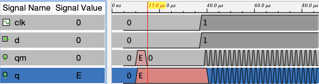
When clock transitions from low to high and data bit transitions from low to high at the same moment, it takes new D=1 to reach to the top NAND gate faster than the negated clock signal, leading the master latch to stay transparent and update \(Q_m\) with value 1. Then the high clock signal is propagated through the slave latch, updating its value with the master latch’s output, i.e., \(Q = Q_m = 1\) as opposed to \(Q = 0\). So, what we have observed here is the following: unless we make the data bit stable a little after the rising clock edge, the slave latch will be updated with the wrong value. This is known as the hold time constraint: how much time we should hold the D input stable for the flip-flop to function as intended.

Here is another case: when (1) the clock transitions from low to high and (2) the data bit D transitions from high to low and (3) \(Q_m\) is previously high, even though the intended behavior is to store D=0 in \(Q\), the negated clock signal and the negated D may or may not reach the bottom NAND gate in the master latch at the same time causing that NAND to output 0 or 1 “randomly”. This will cause \(Q_m\) to fluctuate between 0 and 1, and this is known as metastable state for the memory unit. Metastability of master latch will also lead to the metastability of the slave latch, and therefore, the whole D flip-flop will become metastable as the result. This is illustrated on the timing diagram above.
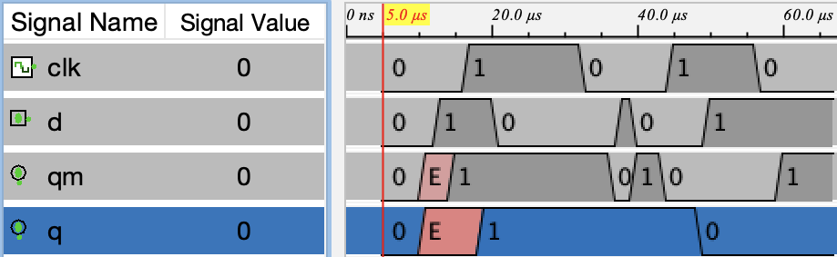
The timing diagram above depicts the behavior of a D flip flop when the setup and hold times are well respected. Having this intuition about these two timing constraints, let’s formalize this framework.
5.5.1 Setup Time Constraint
Imagine the basic but very essential flip-flop setup as shown below:
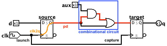
Note that \(t_\text {clk}\) is the clock period, \(t_\text {clk2q}\) is the time it takes for the clock signal to reach the output of the flip-flop, Q. \(t_\text {pd}\) and \(t_\text {cd}\) are the respective propagation and contamination delays of the combinational circuit in between the flip-flops. This being clarified, suppose that the clock signal reaches the left flip-flop at time \(T_\text {launch}\) and the right flip-flop at time \(T_\text {capture}\). Then we say that the following inequality must hold:
Let me try to explain the inequality above. As the clock signal reaches the left (source) flip-flop at \(T_\text {launch}\), it takes \(t_\text {clk2q}\) amount of time for it to affect source \(Q\) output and another \(t_\text {pd}\) amount of time to pass through the combinational circuit (in the worst case scenario). We know that the next clock edge will reach the right (target) flip-flop at time \(T_\text {capture} + t_\text {clk}\), and therefore, the output of the combinational circuit (this value is propagated only after \(T_\text {launch} + t_\text {clk2q} + t_\text {pd}\)) must be stable at least \(t_\text {setup}\) amount of time before the next clock edge reaching the target flip-flop. Since the output of the combinational circuit must be ready before \(T_\text {capture} + t_\text {clk} - t_\text {setup}\), we say \(T_\text {launch} + t_\text {clk2q} + t_\text {pd} \leq T_\text {capture} + t_\text {clk} - t_\text {setup}\).
5.5.2 Hold Time Constraint
Here is the same picture for the hold time constraint, except that here we only care about the shortest path that the signal takes to propagate through the combinational circuit in between the two flip-flops:
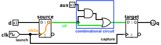
Here is the inequality for the hold time constraint:
Let me now try to explain this inequality. After making sure that the setup time is constraint is not violated, we then also have to check if the output of the combinational logic will stay the same for enough time period (a.k.a. \(t_\text {hold}\)) after the clock edge. As the clock edge reaches the source flip-flop at \(T_\text {launch}\), then takes \(t_\text {clk2q}\) time to affect the its output, and \(t_\text {cd}\) minimum amount of time to pass through the combinational circuit, we say that the new value at the output of this combinational circuit must be ready not before than \(T_\text {capture} + t_\text {hold}\) (when the clock edge reaches the target flip-flop + a little bit of time so that hold time is not violated).
Chapter 6
Let’s Build a Computer!
Congratulations! You have made this far, and now you get to understand and even build a custom 8-bit computer on your own through some guidance provided in this chapter. However, it is important to talk about the instruction set architecture or ISA before building anything. ISA is essentially a sheet of paper that lists all of the basic operations that can be carried in our hypothetical computing machine by providing the instructions in binary directly to the machine. Basically, it is the design process of a computer in a higher level abstraction, which then leads to relatively lower level microarchitecture (how the operations listed on the ISA specification are executed step-by-step) design, and then to gate-level construction of the real physical computer. Here’s the first step of this high-level design process – I would like to represent each instruction in 16 bits or 2 bytes as follows:
| \(b_{15}\) | \(b_{14} b_{13} b_{12} b_{11}\) | \(b_{10} b_9 b_8\) | \(b_7 b_6 b_5 b_4 b_3 b_2 b_1 b_0\) | |||||||
| instruction opcode |
|
|
|||||||
The representation above explains the semantic division of the 2-byte instruction. The MSB (most significant bit) \(b_{15}\) indicates whether instruction is an ALU instruction (such as adding two numbers, logical AND, logical OR, and so on) or memory instruction (such as storing a number in memory, loading values from memory to registers, and so on). The next 4 bits \(b_{14:11}\) is the operation code or opcode that specifies which instruction we want our CPU to execute. Then comes the next 3 bits \(b_{10:8}\) as the first argument of our instruction (\(b_{15:11}\)), which is always going to be a register address in the register file consisting 8 registers. The second byte \(b_{7:0}\) is the second argument, which can be an immediate value or an 8-bit memory address depending on the context/instruction. Since we allow only the second byte of the instruction to work with the memory addresses, fixing 8 bits for this purpose also limits how big of a memory we can possibly work with in this kind of architecture. Since we also want byte-addressable memory system in which one can access the individual bytes by providing an 8-bit address, of course, the answer is we are going to work with \(2^8 = 256\) byte memory. Each of 256 locations is going to represent one byte or 8 bits instead of a single bit. If we wanted to access the individual bits, then the memory would be called bit-addressable and not byte-addressable.
Lastly, since this is going to be an 8-bit computer (byte-addressable memory, support for operations on byte-long numbers, byte-long bus width; in other words, only 8 bits can be travelling accross wires at a given moment), I will call this computer Dummy x8 or Dx8!
6.1 Instruction Set Architecture
One popular architecture for modern computing devices has been Von Neumann architecture. This architecture is essentially the one that mentions a central processing unit or CPU which works with a memory unit where the data and the program is mixed. The CPU consists of a control unit and arithmetic and logic unit or ALU. Control unit is used to orchestrate different components within the CPU and even memory units to some extent. ALU is the part where numbers get crunched and calculations happen. Besides, there is external input and output devices that can be connected to this core computing device (CPU + Memory).
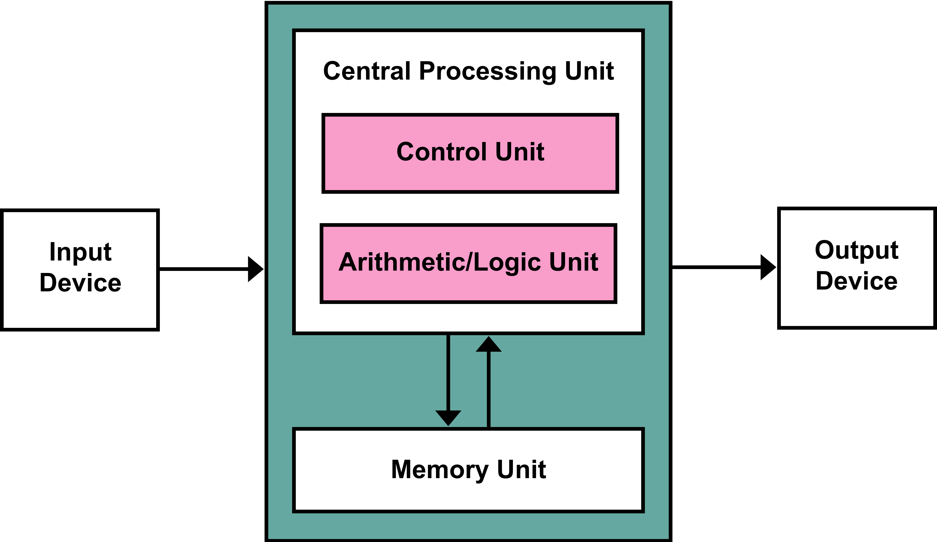
Now, let’s start designing our own ISA from scratch. Just keep in mind that, we will build computer around the architectural principles of Von Neumann’s, however, our instruction set and the microarchitecture (technical gate-level details) will be built and customized for our personal liking. Von Neumann architecture, as illustrated in the figure above, tells us which high-level components there are and how they are frankly connected; it does not dictate how these components ought to be built or which instructions should they be able to carry out. So, we are free to do what the hell we want with this. Nice, let’s get to it!
I visualize the general organization of the DX8 computer as follows:
-
There is a CPU, which has a Control unit and Arithmetic unit (to perform \(a + b\), comparison \(a < b ?\), etc.) + Logic unit (to perform \(a \operatorname {AND} b\), \(\operatorname {NOT} a\), etc.) and a bunch of registers (R0, …, R7 – also known as Register file);
- Controller;
- ALU;
- Register File;
- There is more general non-volatile memory unit – also known as Random Access Memory or RAM, whose bytes can be accessed(read or written) by providing arbitrary 8-bit address;
-
External input unit:
- 8 ON/OFF switches (acting as a “keyboard”) to set the data to be written to the RAM;
- 8 ON/OFF switches to set the memory address;
- Write button to make the computer write the given data into the indicated memory address;
- Reset switch to restart the computer.
Here’s how I visualize this in my mind:
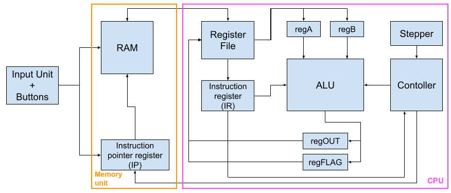
With this high-level visualization of the DX8 computer in mind, let’s see my “beautiful” ISA:
| Mnemonic | Opcode | Semantics |
| load | 0,0000 | \(\texttt {regX} \leftarrow \texttt {memAddr}\) |
| store | 0,0001 | \(\texttt {memAddr} \leftarrow \texttt {regX} \) |
| move | 0,0010 | \(\texttt {regX} \leftarrow \texttt {val}\) |
| arg1 | 0,0011 | \(\texttt {regA} \leftarrow \texttt {regX}\) |
| arg2 | 0,0100 | \(\texttt {regB} \leftarrow \texttt {regX}\) |
| cmp | 1,0000 | \(\texttt {regOUT} \leftarrow \texttt {CMP regA regB}\) |
| add | 1,0001 | \(\texttt {regOUT} \leftarrow \texttt {regA} + \texttt {regB}\) |
| neg | 1,0010 | \(\texttt {regOUT} \leftarrow \text {NOT regA} + 1\) |
| and | 1,0011 | \(\texttt {regOUT} \leftarrow \texttt {regA AND regB}\) |
| or | 1,0100 | \(\texttt {regOUT} \leftarrow \texttt {regA OR regB}\) |
| xor | 1,0101 | \(\texttt {regOUT} \leftarrow \texttt {regA XOR regB}\) |
| not | 1,0110 | \(\texttt {regOUT} \leftarrow \texttt {NOT regA}\) |
| rotl | 1,0111 | \(\texttt {regOUT} \leftarrow \texttt {regA[6:0]\_regA[7]}\) |
| rotr | 1,1000 | \(\texttt {regOUT} \leftarrow \texttt {regA[0]\_regA[7:1]}\) |
| shiftl | 1,1001 | \(\texttt {regOUT} \leftarrow \texttt {regA[6:0]\_0}\) |
| shiftr | 1,1010 | \(\texttt {regOUT} \leftarrow \texttt {0\_regA[7:1]}\) |
| jmp | 0,0101 | \(\texttt {regIP} \leftarrow \texttt {val}\) |
| jmpgt | 0,0110 | \(\texttt {regIP} \leftarrow \begin {cases} \texttt {val}, \text {if gt flag is set} \\ \texttt {regIP} + 1, \text {otherwise} \end {cases}\) |
| jmplt | 0,0111 | \(\texttt {regIP} \leftarrow \begin {cases} \texttt {val}, \text {if lt flag is set} \\ \texttt {regIP} + 1, \text {otherwise} \end {cases}\) |
| jmpeq | 0,1000 | \(\texttt {regIP} \leftarrow \begin {cases} \texttt {val}, \text {if eq flag is set} \\ \texttt {regIP} + 1, \text {otherwise} \end {cases}\) |
Table 6.2 is a very basic and naive instruction set that I have designed for the DX8 computer. Let’s now try to build some of the components that are needed for our CPU. For example, ISA mentions that one should be able to execute add instruction, which performs \(\texttt {regOUT} \leftarrow \texttt {regA} + \texttt {regB}\). So, the plan is to build a subunit called Arithmetic (sub)Unit, and Logic (sub)Unit, then combine them in a single unit called ALU. Let’s see how we can do this.
6.2 Arithmetic
Suppose I wanted to add two 1-bit inputs in1 and in2. What I would like is to build a circuit that gives me their sum in a single bit, as well as their carry (in case the sum does not fit in a single bit). Such as circuit is called half adder and its truth table can be given as follows:
| in1 | in2 | sum | carry | in1 + in2 = [carry][sum] |
| 0 | 0 | 0 | 0 | 00 |
| 0 | 1 | 1 | 0 | 01 |
| 1 | 0 | 1 | 0 | 01 |
| 1 | 1 | 0 | 1 | 10 |
This is obviously very simple truth table, and therefore, the circuit for the half adder can be built as given below:
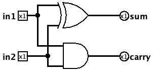
The unfortunate thing about the half adder is that we cannot stack a bunch of these half adders to add two multiple-bit numbers, say \(x_{7:0}\) and \(y_{7:0}\). The reason is obvious if you think about it for a second: because we have to use the carry output of the rightmost bits \(a_i + b_i\) while adding the bits on the left \(x_{i+1} + y_{i+1}\). To do this, we should build a full adder that is capable of adding two 1-bit numbers while also adding another carry input. Therefore, a full adder is essentially a 3-bit adder that outputs 1-bit sum and 1-bit carry-out. Here’s the truth table for it:
| \(\text {carry}_{i}\) | \(x_{i+1}\) | \(y_{i+1}\) | \(\text {sum}_{i+1}\) | \(\text {carry}_{i+1}\) | \(\text {carry}_i + x_{i+1} + y_{i+1} = [\text {carry}_{i+1}][\text {sum}_{i+1}]\) |
| 0 | 0 | 0 | 0 | 0 | 00 |
| 0 | 0 | 1 | 1 | 0 | 01 |
| 0 | 1 | 0 | 1 | 0 | 01 |
| 0 | 1 | 1 | 0 | 1 | 10 |
| 1 | 0 | 0 | 1 | 0 | 01 |
| 1 | 0 | 1 | 0 | 1 | 10 |
| 1 | 1 | 0 | 0 | 1 | 10 |
| 1 | 1 | 1 | 1 | 1 | 11 |
With a little bit of SoP/PoS magic, it is easy to realize the following implementation for the full adder:
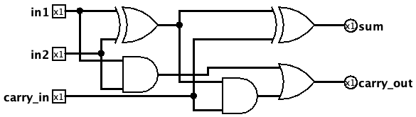
In order to add two 4-bit numbers \(x_{3:0}\) and \(y_{3:0}\), we can stack up 4 full adders as follows:
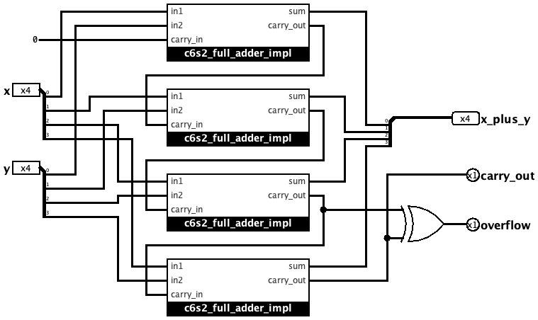
I think it is hopefully pretty obvious how we could scale this up to 8 bits or even further. For our computer, we only need 8-bit adder, so we will stack 4 more full adders on top of the ones shown above and we will call it a day!
6.3 Logic
Performing basic logic on input(s) is much more easier because this is what the logic gates, such as AND, NOT, OR, do by default. All we need to do to scale these logical operations from 1-bit inputs to 8-bit inputs. Doing this is very easy and trivial: given two 8-bit inputs \(x_{7:0}\) and \(y_{7:0}\), connect each bit \(a_i\) and \(b_i\) to a different AND/OR/XOR gate \(G_i\), then the final 8-bit output is the concationation of the outputs of these gates, \(\overline {G_7 \dots G_0}\).
What about comparing two 1-bit numbers? Well here is a pretty intuitive implementation of 1-bit comparator:
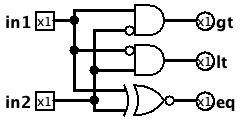
If you wonder how you can build it, just remember that the first step is to write down the truth table for the comparator. My stupid truth table for the circuit above looked like this:
| in1 | in2 |
|
|
|
||||||
| 0 | 0 | 0 | 0 | 1 | ||||||
| 0 | 1 | 0 | 1 | 0 | ||||||
| 1 | 0 | 1 | 0 | 0 | ||||||
| 1 | 1 | 0 | 0 | 1 | ||||||
If we wanted to extend this circuit to compare 4-bit numbers instead, we could do it by stacking up a bunch of these simpler 1-bit comparator units and adding some extra logic that I will leave for you to figure out on your own as an exercise. But here is the circuit for comparing two 4-bit numbers:
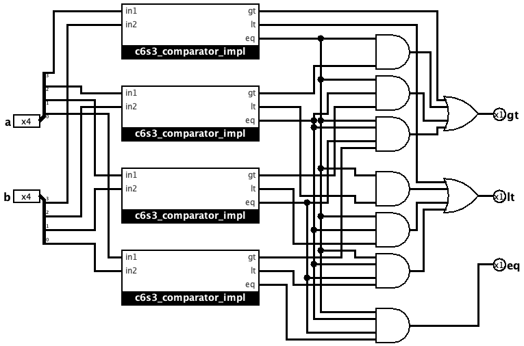
Scaling this further to 8-bit number comparison, the same simple logic follows. Try to do this yourself to see what I mean.
6.4 Arithmetic Logic Unit (ALU)
Now that we have built both arithmetic unit and logic unit, we can combine them under the arithmetic and logic unit. Moreover, we will add some more functionality to this ALU bad boy. Here are the things I want my ALU to be capable of doing:
- Rotate a number to left or to right by one bit (rotl and rotr): \(\operatorname {rotl}(\overline {a_7 a_6 \dots a_1 a_0}) = \overline {a_6 a_5 \dots a_1 a_0 a_7}\) and \(\operatorname {rotr}(\overline {a_7 a_6 \dots a_1 a_0}) = \overline {a_0 a_7 a_6 \dots a_2 a_1}\).
- Shift a number to left or to right by one bit (shiftl and shiftr): \(\operatorname {shiftl}(\overline {a_7 a_6 \dots a_1 a_0}) = \overline {a_6 a_5 \dots a_1 a_0 0}\) and \(\operatorname {shiftr}(\overline {a_7 a_6 \dots a_1 a_0}) = \overline {0 a_7 a_6 \dots a_2 a_1}\).
- 2’s complement of a number: NOT(a) + 1.
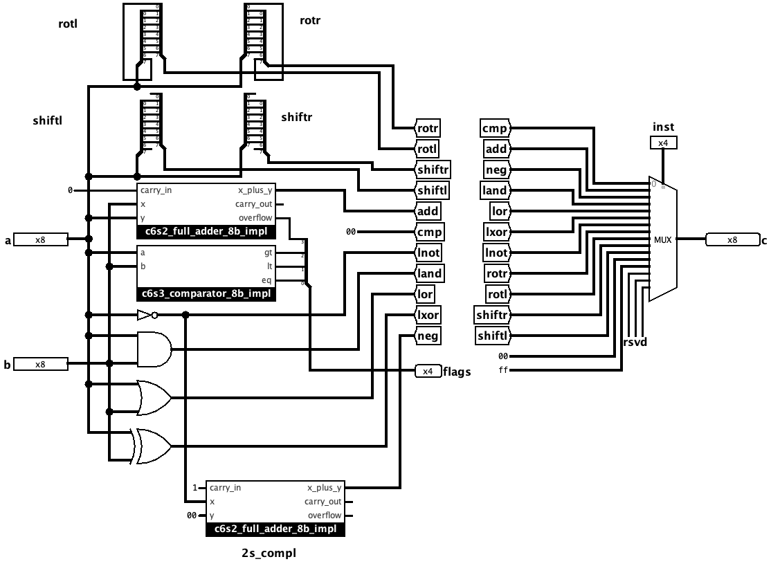
Since our ISA has assigned special opcodes for each operation, we connect outputs of these arithmetic and logic components (such as rotl, rotr, shiftl, shiftl, 8-bit adder, 8-bit comparator, NOTx8, ANDx8, ORx8 XORx8, 2’s complementer) to a 16x1 MUX and provide the 4-bit opcode (\(b_{14:11}\)) as the selector bits.
6.5 Random Access Memory (RAM)
Having learned about the latches and flip-flops, building an 8-bit register is easy: just stack 8 flip-flops (or latches if you don’t want edge-triggered memory). Since we want edge-triggered memory, here is a simple implementation by using 8 D flip-flops, all in sync with the global clock:
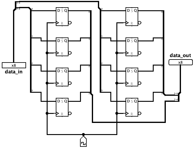
We will come back to this 8-bit register in a bit. Now, let’s understand how addressing works in a basic bit-level addressable memory. Say there are 4 D flip-flops (conventionally indexed from 00 to 11 in binary) and we would like to ”use” the third one (at index 10). By ”using”, we have to also specify whether we would like to write some data to it or read the data already stored in it. Therefore, we have two additional input bits WE (write-enable) and RE (read-enable). Sometimes these are also called load and enable bits. Here is the circuit that allows us to work with such a memory unit:
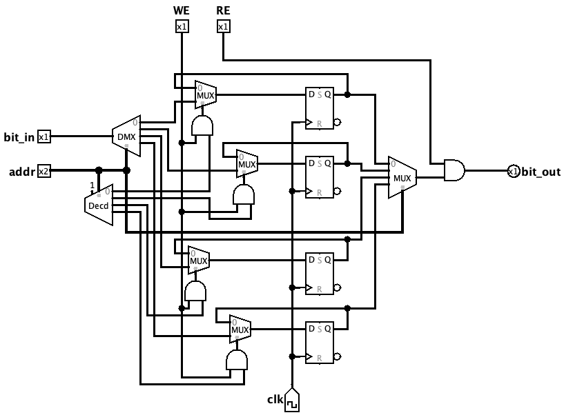
Now, let’s go back our 8-bit register once again. This is essentially what byte-addressable memory uses: we stack up 256 of these 8-bit registers and only active one of them depending on the 8-bit address, as well as WE/RE bits. We used four 2x1 MUXs to select one out of 4 D flip-flops previously. It is easy to apply the same logic to select one out of 4 8-bit registers, as well. This will give us 4 bytes of byte-addressable memory unit or 2x8 RAM (2 indicates number of address bits and 8 represents addressability). To construct 4x8 RAM, you would need to apply the same logic using four 2x1 MUXs recursively to four 2x8 RAM units (instead of four D flip-flops). Then to build 6x8 RAM, the same organization of 2x1 MUXs will be connected to four 4x8 RAM units. Finally, by using four 6x8 RAM units in a similar organization, we could build 8x8 RAM or 256 byte byte-addressable RAM.
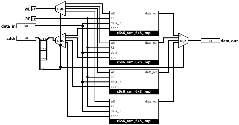
The figure above shows the construction of 8x8 RAM by using four 6x8 RAM units, each of which is similarly constructed by using four 4x8 RAM units (this goes on until we use four 8-bit registers to construct a 2x2 RAM unit).
6.6 The DX8 Computer
We are going to build the four high-level components that we are going to use to assembly my DX8 computer. These components are the following:
- Stepper - that turns on a single output bit in a predefined order repetitively and synchronously based on the global clock signal.
- Register File - a small memory unit consisting of 8 registers that can be selected by using 3-bit addresses, also in sync with the clock.
- ALU - we have already built this; we are just going to containarize it.
- Contoller - that output the control bits for different components inside our computer depending the current workflow, syncronized with the clock.
It is very natural to ask why the hell we need a thing called stepper in the first place. Well, to understand the reason we need it, I first need to introduce the four main stages of computation that goes inside a computer:
- Fetch - in this stage Controller sets the RE control bits of RAM to read data, and sets the WE control bits of Register file and other bunch of relevant registers (such as IR) so that instruction is fetched and saved into the registers properly for the next stage;
- Decode - in this stage the instruction is scrutinized to understand whether it’s ALU or Memory instruction, and which component within ALU is responsible for it;
- Execute - in this stage the decoded instruction is executed either in ALU or elsewhere and the outputs are stored temporarily in registers such as regOUT, regFLAG, etc.;
- Load - in this stage the temporarily saved results from the previous stage gets written back to the main memory unit (RAM) if needed, and cycle repeats again.
There are different ways of going through these 4 stages inside computers in general. Here are 3 different ways that a computer can be built to go through these Fetch-Decode-Execute-Load stages:
- Single-cycle processing uses single clock cycle to go through all of the 4 stages at once.
- Multi-cycle processing uses different clock cycles to go through each of 4 stages individually, improving the performance compared to a single-cycle machine.
- Pipelined processing further imporoves the performance of a multi-cycle CPU by not putting the next instructions throught the idle stages not used by the current instruction anymore.
If you do not fully understand what pipelining is, do not worry about it too much for now. I have decided that I want to go with multi-cycle processor design for the DX8 CPU. You can view it as a tradeoff for performance and simplicity for this book. Building single-cycle is the simplest and the pipelined is the hardest, while single-cycle is the least efficient and the pipelined is the most efficient. This leaves the multi-cycle CPU in the middle: moderate complexity in design and moderate performance in practice! That’s what I wanted.
6.6.1 Single-cycle, Multi-cycle, Pipelined Design
We said there are 4 stages of electricity running inside our computer: (1) electricity running to fetch instruction from main memory to the instruction register IR, (2) electricity running to decode the fetched IR content to know what control signals should be sent to the rest of the hardware to execute the instruction in IR, (3) electricity running to actually follow the generated control signal to the different hardware components in order to execute the instruction and save results into their corresponding registers, (4) electricity running to store these results held in temporary registers into the main memory if needed. Well, having 4 stages like this makes the design process easier and modular. Here is the roughly drawn picture illustrating these 4 stages in a single-cycle and multi-cycle processor:
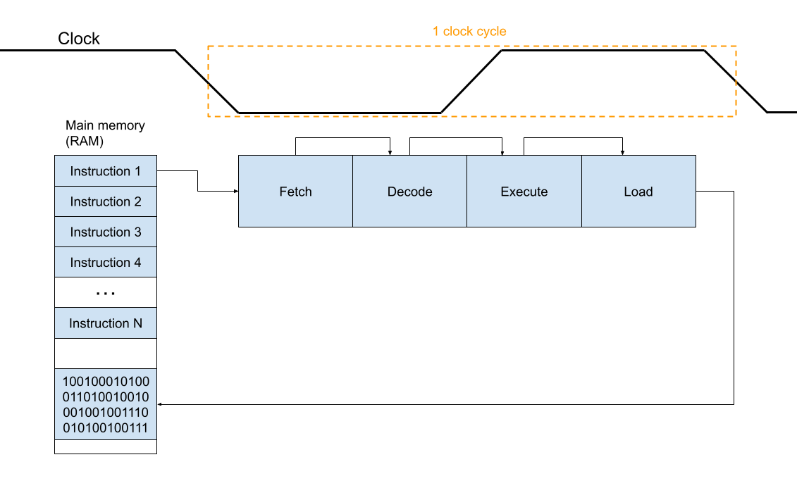
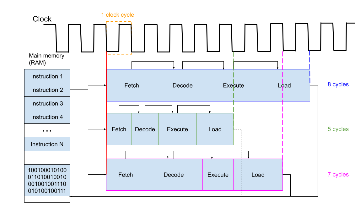
In a pipelined processing, the unused stages by the current instruction is given to the use for the next instruction. This makes the next instruction to already start executing even when the previous instruction is not completely finished with all the stages. This is shown in the figure below clearly:
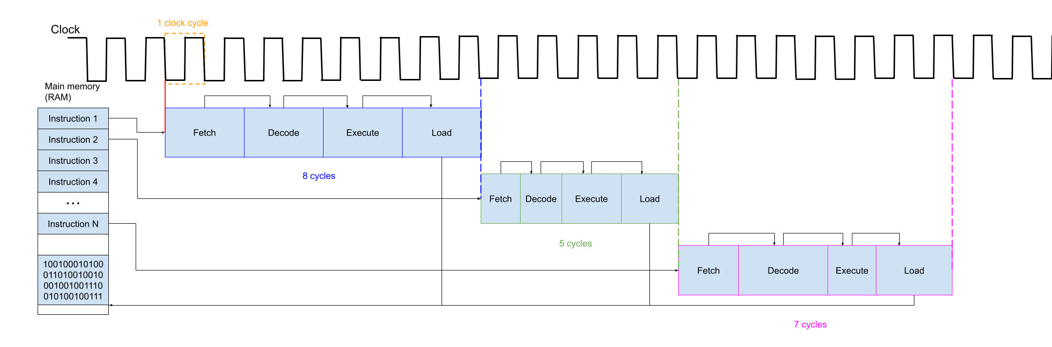
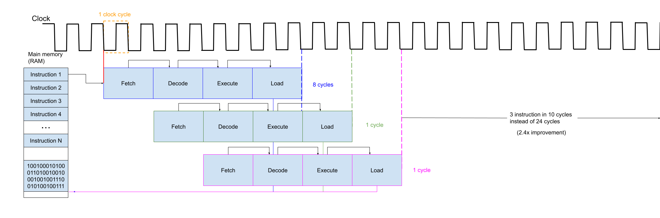
Speaking of optimizing CPU performance, here is something that I want to mention very briefly for the curious readers out there. The amount of time it takes for the CPU to finish one instruction is called latency, and the number of instructions finished in each “second” is called throughput. Moving from single-cycle to multi-cycle processor design clearly improves performance by reducing the latency, and moving from multi-cycle to pipelined processor does not inherently change the latency (that is, an instruction still takes the same 4 stages in multiple cycles to finish) but increases the throughput. This can be clearly observed from the figure above as follows:
- If the longest instruction takes 100 ns then the clock period must be at least 100 ns in single-cycle CPU in order to finish even the hardest instruction properly;
- In a single cycle CPU, setting clock period to 100 ns will also cause every instruction to finish in 100 ns (even if some instruction could have been finished sooner than that);
- Multi-cycle CPU solves this problem by allocating varying number of cycles for each stage in Fetch-Decode-Execute-Load; now, if an instruction could be fetched in 2 cycles then only 2 cycles are spared for it, and if a single cycle is enough for decoding then only single cycle is spared for decoding, and so on;
- However, the next instruction must wait for the current one to completely finish in multi-cycle CPU; but if current instruction has already finished the Fetch stage and now is processed in the Decode stage, why shouldn’t we allow the next instruction to be fetched since our “fetcher” is idle?
- Pipelined CPU solves this problem by pipelining instructions next to one another, increasing the throughput.
Even though the latency does not change when we go from multi-cycle CPU to pipelined one (see the diagram above again – clock period is the same for both), in multi-cycle design it would take 24 cycles to execute 3 instructions (assuming each phase takes exactly 2 cycles, and therefore, each instruction takes exactly 8 cycles), whereas in pipelined design it would take 10 cycles for the same 3 instructions to finish. In this example, throughput for the multi-cycle CPU would be \(\frac {3}{24} = 0.125\), and for pipelined CPU it would be \(\frac {3}{10} = 0.3\); this is 2.4x more throughput… 2.4x more instructions per cycle.
6.6.2 Stepper
To have a clear separation of which phase is executing for a given instruction, we are going to build a component called stepper. Stepper has one external reset input. It operates with the clock signal to output one-hot encoded values to indicate which stage the CPU should be in the current clock cycle. To build a stepper, we can use a binary counter and a decoder as follows:
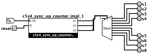
To build DX8, I am going to allocate maximum of 2 steps (or 2 clock cycles) for each stage. Therefore, Fetch will take 2 clock cycles (steps 1 and 2), Decode will take the next 2 clock cycles after Fetch (steps 3 and 4), Execute will take the next 2 clock cycles (that is steps 5 and 6), and Load will take the last 2 clock cycles (steps 7 and 8). Notice that the stepper will go from step 1 to step 8, and then it will go back to step 1 again, and the same behavior will repeat. This is literally what stepper is useful for: for telling us which stage we are in currently.
Before ending this section, let me briefly show you another pair of useful components that are going to be used in DX8: register file with 8 8-bit registers and 8-bit ALU. Designing the register file is really easy since we have already seen how RAM is built. We will use the same logic to build 3x8 RAM (byte-addressable RAM with 3-bit addresses):
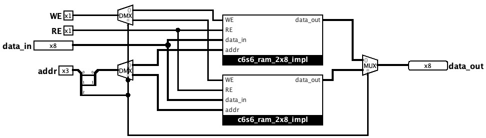
The register file built in the figure above actually holds 16 registers, but we will only use the first 8 of them. Now, let’s see our ALU component that we built previously but did not “containarize” it.

There you go. We have a 8-bit ALU component as well as the register file.
6.6.3 Controller
We need to build the last component before we put everything together for my DX8 computer. The component we are going to build is called Control Unit or Controller. But you may wonder why we need such a component in the first place. Let me explain.
Suppose we are in the first stage where we need to fetch an instruction from the main memory into the instruction register IR. The question is, which wires are going to be active during this stage? To be able to answer this question, let’s see the data path of the DX8 computer that I gave you earlier:
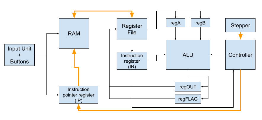
When decoding the arguments present in the instruction must be sent to their corresponding register regA and regB and the operation must be sent in 4-bits to the ALU, assuming it is an ALU instruction. Therefore, the data path for decoding should roughly look like something below:
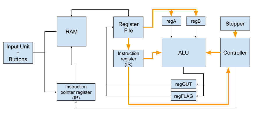
Assuming we are executing an ALU instruction, the wires connecting two operands regA and regB to the ALU (because ALU will be reading inputs from these registers), the wire connecting IR to ALU (because ALU will output the result of the operation corresponding to the instruction held in the IR), the wires connecting ALU to the temporary output registers regOUT and regFLAG (because ALU ouput will be stored in these registers), and a bunch of wires connected/connecting the Controller (because Controller decides these control signals that I mentioned based on the context, such as Stepper’s output and IR’s content) on the datapath will need to become active. The active wires are shown with orange color in the figure below:
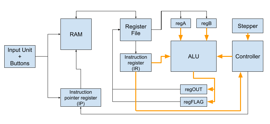
Finally, the load or write-back stage may require regOUT and regFlAG content to be moved into the register file, or some register’s content in the register file to be stored in the RAM by providing an address from the IP. This is illustrated in the figure given below:
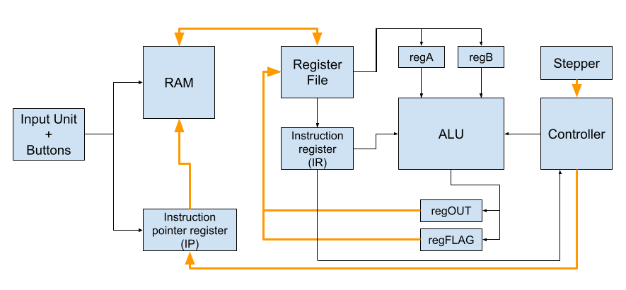
Now that we know what wires become “hot” during each and every stage of clock cycles, how do we make these wires become “hot” and active? Well, we do it by basically read-enabling outputs of a source component and write-enabling the target component that the data needs to transfer to. Controlling these read-enable, write-enable, or some of the select bits of MUXs used to transfer data is the job of controller. The controller takes signal from various sources, important one being the stepper’s output to know which stage is executing and the instruction itself, and decides which enable/select bits must be turned on and off for other components.
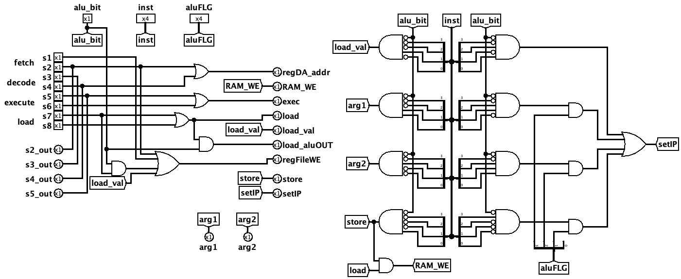
Above you see the implementation of the control unit that is used in DX8. It is not too fancy: if you take a look at it closely, you will be able to figure it out easily. For example, look at what happens when controller’s s1 input becomes high: regFileWE turns high (which is connected to the write-enable input of the register file), allowing the instruction to be copied from the main memory to the register file during the first cycle of fetching. The inputs and outputs of the controller will make sense once you see all the components together inside the DX8 computer. That’s when you will be able to track each output and wire to see which components get affected by the control outputs. So, let’s see the whole thing!
6.6.4 Putting everything together!
Here is the 8-bit Dummy computer:
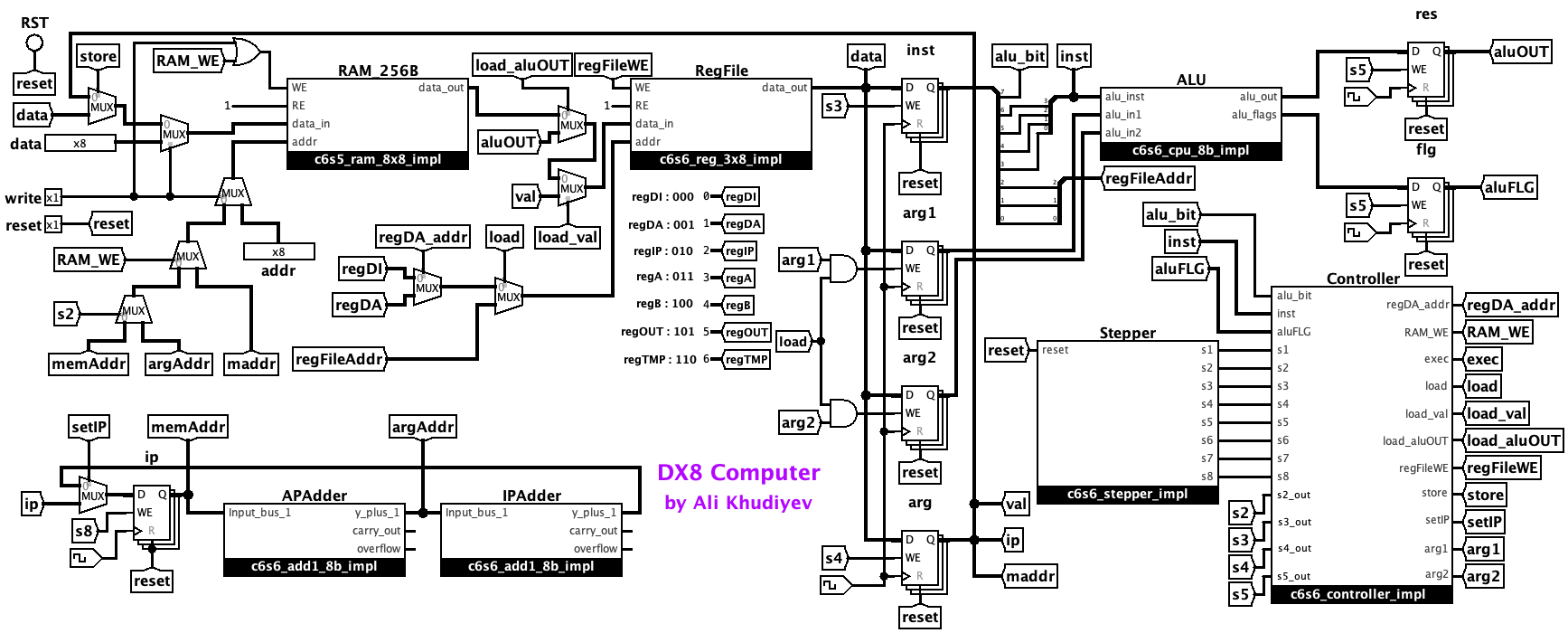
It even has very basic keyboard: 8-bit data input switches and 8-bit addr address switches (with which you can specify the memory address inside RAM you want to put your input data). Before I explain how input system works for this computer, let me first tell you the difference between a (push) button and a switch. A button sends high signal through its output wire as long as it is pressed; its output immediately drops to 0 when you lift your finger up. In contrast, a switch becomes ON (sends high signal through its output wire) once you turn it on, and then you can keep your fingers away from it and it will still keep sending 1 through the wire; it will become OFF again once you turn it off and then it will stay OFF unless you turn it on again later on. The difference may sound subtle, but it is important: to make push button become ON (to send high signal) you need to actively use your finger to press it, whereas you only need your finger once to turn on the switch. Having clarified this difference between these two essential input components, this is how you can operate the DX8 computer:
- Turn on the single-bit reset switch.
-
If you want to program the computer before letting it run:
- Put in the data bits in the 8-bit data switch.
- Put in the address bits in the 8-bit addr switch.
- Push the write button (it is essentially the same as turning on 1-bit switch and then turning it off instantly).
- Repeat this process as long as you haven’t finished putting everything you need in the main memory.
- Turn off the reset switch and the DX8 will start working.
I hope you enjoyed reading this book. You can find everything related to DX8 in the following github repo: dx8-course-material.
Chapter 7
Epilogue
You have reached the end of this journey. Thanks for reading this unpolished draft book, which is more like a lecture notes from the caveman. I want you to know that any constructive feedback is appreciated. You can contact me via my email for this. Now, if you are a sharp reader you may catch a lot of things and technical details which were introduced and explained in a very hand-wavy manner. This is no coincidence. I wanted to keep this book under 100 pages, so that readers with even a little patience could get the courage to read it without hesitation. That’s why I have usually went straight to the point sometimes without trying to explain very thoroughly the whys, hows, and whats. What you may also notice is that while building my DX8 computer, I did not bother with the timing constraints at all, even though I was telling you to be careful about all this setup and hold time constraints while building sequential circuits. The reason I did not bother the timing in parts of the book where I was explaining how DX8 can be built is because real computer architects do not care about timing violations. If it works, then it works; and if it doesn’t then you suck and you need to probably go back to checking your timing constraints after making sure your logic works right. Okay, jokes aside, I did not do the time checks while building DX8 because I left it as an exercise for readers. Okay, okay… I just didn’t because I did not want to bother (at least for now… or maybe for ever…).